| Chemical Formula | NiSb |
| Catalog No. | ST0941 |
| CAS Number | 12035-52-8 |
| Purity | 99.9%, 99.95%, 99.99%, 99.995%, 99.999% |
| Shape | Discs, Plates, Column Targets, Step Targets, Custom-made |
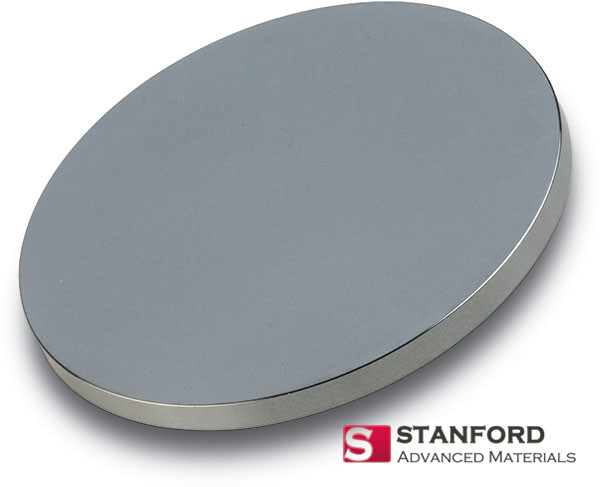
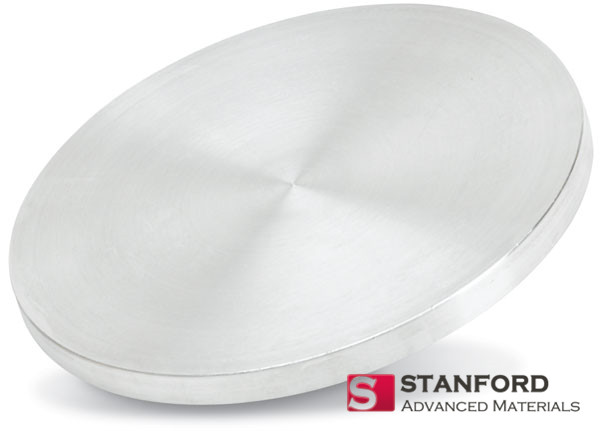
The Nickel Antimonide Sputtering Target is available in various forms, purities, sizes, and prices. Stanford Advanced Materials (SAM) is a trusted industry leader with a proven track record in delivering high-purity Nickel Antimonide Sputtering Targets at competitive prices.
Nickel Antimonide Sputtering Target is a specialized material used in the sputtering process for thin film deposition. Nickel antimonide is a semiconductor material. Thin films of NiSb deposited using sputtering targets can be used in various semiconductor applications.
Stanford Advanced Materials (SAM) specializes in creating Nickel Antimonide Sputtering Targets with optimal density and minimal average grain size. By utilizing the sputtering technique, we can deposit ultra-high purity thin films of sputtered metal or oxide materials onto a solid substrate. The exceptional purity of our targets ensures the superior quality and performance of the resulting film.
Related Product: Nickel Silicide Sputtering Target, Nickel Oxide Sputtering Target
| Compound Formula | NiSb |
| Molecular Weight | 180.45 |
| Appearance | gray target |
| Melting Point | 1102℃ |
| Density | 8.56 g/cm3 |
| Available Sizes | Dia.: 1.0″, 2.0″, 3.0″, 4.0″, 5.0″, 6.0″
Thick: 0.125″, 0.250″ |
Our Nickel Antimonide Sputtering Target is carefully handled during storage and transportation to preserve the quality of our products in their original condition.
SAM’s Nickel Antimonide Sputtering Target is available in various forms, purities, and sizes. We specialize in producing high-purity physical vapor deposition (PVD) materials with the highest possible density and smallest possible average grain sizes for use in semiconductor, chemical vapor deposition (CVD) and physical vapor deposition (PVD) display and optical applications.
Submit your review | |