
A PVT-Robust and 73.9 mHz High-Pass Corner Instrumentation Amplifier with an SCF-SCR-PR Hybrid Feedback Resistor

 ,
,
Abstract
:1. Introduction
2. Design and Analysis of the Proposed Structure
2.1. Theoretical Analysis of the Capacitively Coupled IA
2.2. Circuit Implementation
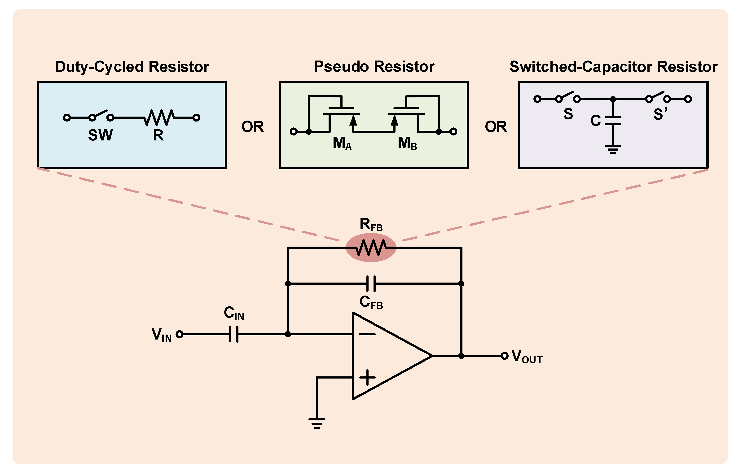
2.2.1. SSP Hybrid Feedback Resistor
2.2.2. Push–Pull Amplifier
2.2.3. The Proposed IA
3. Simulation Results and Discussion
3.1. AMP Results
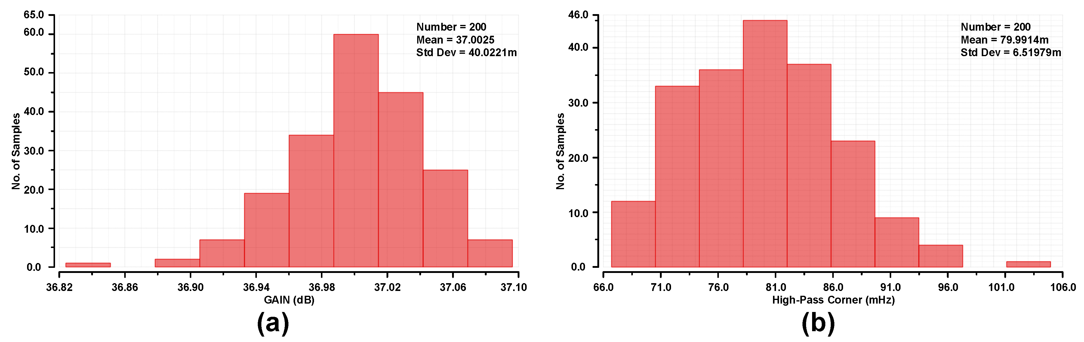
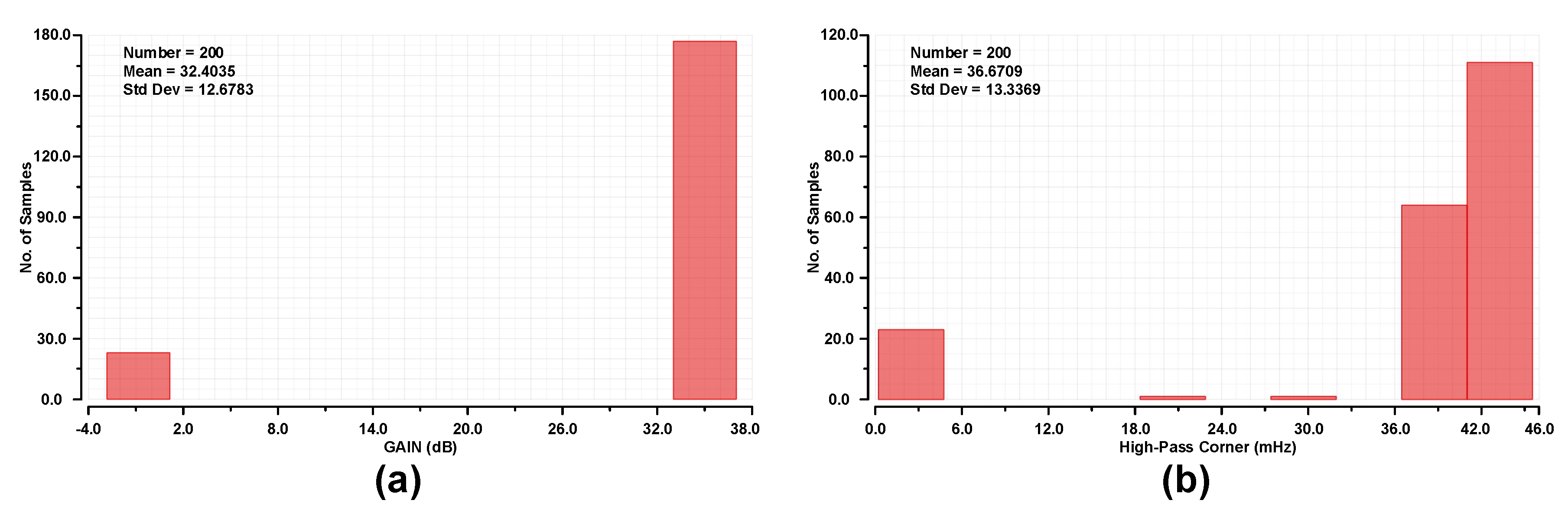
3.2. IA Results
3.3. AFE Results
4. Conclusions
Author Contributions
Funding
Data Availability Statement
Conflicts of Interest
References
- Zhang, C.; Wang, J.; Wang, L.; Liu, L.; Li, Y.; Zhu, Z. High Input Impedance Low-Noise CMOS Analog Frontend IC for Wearable Electrocardiogram Monitoring. IEEE Trans. Circuits Syst. II Express Briefs 2020, 67, 1169–1173. [Google Scholar] [CrossRef]
- Karimlou, A.; Yavari, M. A Low-Power Delta-Modulation-Based ADC for Wearable Electrocardiogram Sensors. IEEE Trans. Circuits Syst. II Express Briefs 2022, 69, 3670–3674. [Google Scholar] [CrossRef]
- Kim, J.; Duan, Q.; Choi, J.; Song, C.; Roh, J. A 2.16-μW Low-Power Continuous-Time Delta–Sigma Modulator with Improved-Linearity Gm for Wearable ECG Application. IEEE Trans. Circuits Syst. II Express Briefs 2022, 69, 4223–4227. [Google Scholar]
- Park, Y.; Cha, J.-H.; Han, S.-H.; Park, J.-H.; Kim, S.-J. A 3.8-μW 1.5-NEF 15-GΩ Total Input Impedance Chopper Stabilized Amplifier with Auto-Calibrated Dual Positive Feedback in 110-nm CMOS. IEEE J. Solid-State Circuits 2022, 57, 2449–2461. [Google Scholar] [CrossRef]
- Zhang, T.; Li, Y.; Su, C.; Zhang, X.; Yang, Y. A 1 V 3.5 μW Bio-AFE with Chopper-Capacitor-Chopper Integrator-Based DSL and Low Power GM-C Filter. IEEE Trans. Circuits Syst. II Express Briefs 2022, 69, 5–9. [Google Scholar] [CrossRef]
- Hsu, Y.-P.; Liu, Z.; Hella, M.M. A 1.8 μW-65 dB THD ECG Acquisition Front-End IC Using a Bandpass Instrumentation Amplifier with Class-AB Output Configuration. IEEE Trans. Circuits Syst. II Express Briefs 2018, 65, 1859–1863. [Google Scholar]
- Liu, L.; Hua, T.; Zhang, Y.; Mu, J.; Zhu, Z. A Robust Bio-IA with Digitally Controlled DC-Servo Loop and Improved Pseudo-Resistor. IEEE Trans. Circuits Syst. II Express Briefs 2020, 67, 440–444. [Google Scholar] [CrossRef]
- Hao, Y.; Chen, M.; Chen, W.; Zhao, Y.; Li, Y. An Active Electrode for Vital Signal Acquisition with Accurately-Tunable Sub-Hz High-Pass-Corner Frequency and 164-mVpp Linear-Input-Range. IEEE Trans. Circuits Syst. II Express Briefs 2021, 68, 1610–1614. [Google Scholar]
- Zhang, S.; Li, Q. An AC-Coupled Instrumentation Amplifier Achieving 110-dB CMRR at 50 Hz with Chopped Pseudoresistors and Successive-Approximation-Based Capacitor Trimming. IEEE J. Solid-State Circuits 2021, 56, 277–286. [Google Scholar] [CrossRef]
- Zhang, S.; Zhou, X.; Gao, C.; Li, Q. A 130-dB CMRR Instrumentation Amplifier with Common-Mode Replication. IEEE J. Solid-State Circuits 2022, 57, 278–289. [Google Scholar] [CrossRef]
- Ng, K.A.; Xu, Y.P. A Low-Power, High CMRR Neural Amplifier System Employing CMOS Inverter-Based OTAs with CMFB Through Supply Rails. IEEE J. Solid-State Circuits 2016, 51, 724–737. [Google Scholar]
- Chandrakumar, H.; Marković, D. A High Dynamic-Range Neural Recording Chopper Amplifier for Simultaneous Neural Recording and Stimulation. IEEE J. Solid-State Circuits 2017, 52, 645–656. [Google Scholar] [CrossRef]
- Harrison, R.R. A low-power, low-noise CMOS amplifier for neural recording applications. In Proceedings of the 2002 IEEE International Symposium on Circuits and Systems. Proceedings (Cat. No.02CH37353), Phoenix-Scottsdale, AZ, USA, 26–29 May 2002; Volume 5, pp. 197–200. [Google Scholar]
- Verma, N.; Shoeb, A.; Bohorquez, J.; Dawson, J.; Guttag, J.; Chandrakasan, A.P. A Micro-Power EEG Acquisition SoC with Integrated Feature Extraction Processor for a Chronic Seizure Detection System. IEEE J. Solid-State Circuits 2010, 45, 804–816. [Google Scholar] [CrossRef]
- Chandrakumar, H.; Marković, D. 5.5 A 2 μW 40 mVpp linear-input-range chopper- stabilized bio-signal amplifier with boosted input impedance of 300 MΩ and electrode-offset filtering. In Proceedings of the 2016 IEEE International Solid-State Circuits Conference (ISSCC), San Francisco, CA, USA, 31 January–4 February 2016; pp. 96–97. [Google Scholar]
- Chandrakumar, H.; Marković, D. An 80-mVpp Linear-Input Range, 1.6-GΩ Input Impedance, Low-Power Chopper Amplifier for Closed-Loop Neural Recording That Is Tolerant to 650-mVpp Common-Mode Interference. IEEE J. Solid-State Circuits 2017, 52, 2811–2828. [Google Scholar] [CrossRef]
- Zou, X.; Xu, X.; Yao, L.; Lian, Y. A 1-V 450-nW Fully Integrated Programmable Biomedical Sensor Interface Chip. IEEE J. Solid-State Circuits 2009, 44, 1067–1077. [Google Scholar] [CrossRef]
- Gan, R.; Lyu, L.; Mu, G.; Shi, C.-J.R. A Neural Recording Analog Front-End with Exponentially Tunable Pseudo Resistors and On-Chip Digital Frequency Calibration Loop Achieving 3.4% Deviation of High-Pass Cutoff Frequency in 5-to-500 Hz Range. In Proceedings of the 2022 IEEE Custom Integrated Circuits Conference (CICC), Newport Beach, CA, USA, 24–27 April 2022; pp. 1–2. [Google Scholar]
- Zhou, Z.; Liao, H.; Zhu, L.; Liu, Y.; Zhu, L.; Wang, K.; Wang, Z. A Bootstrapped Pseudo Resistor by Reusing OTA-C Filter for Neural Signal Processing. IEEE Trans. Circuits Syst. II Express Briefs 2022, 69, 714–718. [Google Scholar] [CrossRef]
- Zhang, F.; Holleman, J.; Otis, B.P. Design of Ultra-Low Power Biopotential Amplifiers for Biosignal Acquisition Applications. IEEE Trans. Biomed. Circuits Syst. 2012, 6, 344–355. [Google Scholar] [CrossRef]
- Park, S.-Y.; Cho, J.; Na, K.; Yoon, E. Modular 128-Channel Δ-ΔΣ Analog Front-End Architecture Using Spectrum Equalization Scheme for 1024-Channel 3-D Neural Recording Microsystems. IEEE J. Solid-State Circuits 2018, 53, 501–514. [Google Scholar] [CrossRef]
- Deguchi, T.; Tanaka, R.; Kawazoe, S.; Fukuoka, R.; Nakano, N. A Low Noise Analog Front-end Design with an N-path Filter for Dry EEG Recording. In Proceedings of the 2018 International Symposium on Intelligent Signal Processing and Communication Systems (ISPACS), Ishigaki, Japan, 27–30 November 2018; pp. 523–526. [Google Scholar]
- Hong, J.-H.; Liang, M.-C.; Haung, M.-Y.; Tsai, T.-H.; Fang, Q.; Lee, S.-Y. Analog front-end circuit with low-noise amplifier and high-pass sigma-delta modulator for an EEG or ECoG acquisition system. In Proceedings of the International Symposium on Bioelectronics and Bioinformations 2011, Suzhou, China, 3–5 November 2011; pp. 17–20. [Google Scholar]
- Tang, T.; Park, J.H.; Zhang, L.; Ng, K.A.; Yoo, J. Group-Chopping: An 8-Channel, 0.04% Gain Mismatch, 2.1 μW 0.017 mm2 Instrumentation Amplifier for Bio-Potential Recording. IEEE Trans. Biomed. Circuits Syst. 2022, 16, 361–371. [Google Scholar] [CrossRef]
- Hsu, Y.-P.; Liu, Z.; Hella, M.M. A −68 dB THD, 0.6 mm2 Active Area Biosignal Acquisition System with a 40–320 Hz Duty-Cycle Controlled Filter. IEEE Trans. Circuits Syst. I Regul. Pap. 2020, 67, 48–59. [Google Scholar] [CrossRef]
- Meng, X.; Li, W.; Temes, G.C. A fully-differential input amplifier with band-pass filter for biosensors. In Proceedings of the 2014 IEEE International Symposium on Circuits and Systems (ISCAS), Melbourne, VIC, Australia, 1–5 June 2014; pp. 21–24. [Google Scholar]
- Chandrakumar, H.; Markovic, D. 27.1 A 2.8 μW 80 mVpp-linear-input-range 1.6 GΩ-input impedance bio-signal chopper amplifier tolerant to common-mode interference up to 650 mVpp. In Proceedings of the 2017 IEEE International Solid-State Circuits Conference (ISSCC), San Francisco, CA, USA, 5–9 February 2017; pp. 448–449. [Google Scholar]
- Abbasi, M.U. A Wearable EEG Amplifier Using a Novel Teraohm Low-Distortion Tunable Hybrid Pseudo-Resistor. In Proceedings of the 2021 IEEE International Symposium on Circuits and Systems (ISCAS), Daegu, Republic of Korea, 22–28 May 2021; pp. 1–5. [Google Scholar]
- Reich, S.; Fritschi, D.; Sporer, M.; Ortmanns, M. An Experimental Reliability Study of Pseudo-Resistors in Biomedical Applications. In Proceedings of the 2022 IEEE International Symposium on Circuits and Systems (ISCAS), Austin, TX, USA, 27 May–1 June 2022; pp. 1892–1895. [Google Scholar]
- Chen, Y.-P.; Jeon, D.; Lee, Y.; Kim, Y.; Foo, Z.; Lee, I.; Langhals, N.B.; Kruger, G.; Oral, H.; Berenfeld, O.; et al. An Injectable 64 nW ECG Mixed-Signal SoC in 65 nm for Arrhythmia Monitoring. IEEE J. Solid-State Circuits 2015, 50, 375–390. [Google Scholar] [CrossRef]
- Bai, W.; Zhu, Z.; Li, Y.; Liu, L. A 64.8 μW > 2.2 GΩ DC–AC Configurable CMOS Front-End IC for Wearable ECG Monitoring. IEEE Sens. J. 2018, 18, 3400–3409. [Google Scholar] [CrossRef]
- Uran, A.; Leblebici, Y.; Emami, A.; Cevher, V. An AC-Coupled Wideband Neural Recording Front-End with Sub-1 mm2 × fJ/conv-step Efficiency and 0.97 NEF. IEEE Solid-State Circuits Lett. 2020, 3, 258–261. [Google Scholar] [CrossRef]
- Fathy, N.S.K.; Huang, J.; Mercier, P.P. A Digitally Assisted Multiplexed Neural Recording System with Dynamic Electrode Offset Cancellation via an LMS Interference-Canceling Filter. IEEE J. Solid-State Circuits 2022, 57, 953–964. [Google Scholar] [CrossRef]


| [26] | [6] * | [25] * | [29] | This Work * | |
|---|---|---|---|---|---|
| Year | 2014 | 2018 | 2020 | 2022 | 2023 |
| Technology | CMOS 180 nm | CMOS 130 nm | CMOS 130 nm | CMOS 180 nm | CMOS 130 nm |
| IA Topology | Cap-Coupled | Cap-Coupled | Cap-Coupled | Cap-Coupled | Cap-Coupled |
| 1 Topology | SCR | PR | PR | PR | SSP |
| Gain | 36.7 dB | 34.6 dB | 55 dB | 52 dB | 37 dB |
| High-Pass Corner | 300 mHz | 702 mHz | 766 mHz | 411.6 mHz | 73.9 mHz |
| High-Pass Corner: Max. − Min. | N/A 2 | 0.82 Hz | 0.86 Hz | 2.6 Hz | 0.06 Hz |
| High-Pass Corner var. Over Temp. | N/A 2 | 8 mHz/°C | 12.5 mHz/°C | 100 mHz/°C | 0.05 mHz/°C |
| [30] | [31] | [32] | [33] | This Work * | |
|---|---|---|---|---|---|
| Year | 2015 | 2018 | 2020 | 2021 | 2023 |
| Technology | CMOS 65 nm | CMOS 180 nm | CMOS 65 nm | CMOS 65 nm | CMOS 130 nm |
| ADC Topology | 8 bit SAR | Delta-Sigma | 10 bit SAR | 10 bit SAR | 10 bit SAR |
| Calibration | NO | NO | NO | NO | YES |
| AFE SNDR | 30.7 dB | 53.2 dB | 50.5 dB | 46.3 dB | 53.9 dB |
| AFE THD | N/A 1 | N/A 1 | 1.1% | <0.146% | 0.03% |
Disclaimer/Publisher’s Note: The statements, opinions and data contained in all publications are solely those of the individual author(s) and contributor(s) and not of MDPI and/or the editor(s). MDPI and/or the editor(s) disclaim responsibility for any injury to people or property resulting from any ideas, methods, instructions or products referred to in the content. |
© 2024 by the authors. Licensee MDPI, Basel, Switzerland. This article is an open access article distributed under the terms and conditions of the Creative Commons Attribution (CC BY) license (https://creativecommons.org/licenses/by/4.0/).
Share and Cite
Xu, H.; Liu, Y.; Duan, Y.; Li, T.; Zhang, J.; Li, Z.; Zhang, H. A PVT-Robust and 73.9 mHz High-Pass Corner Instrumentation Amplifier with an SCF-SCR-PR Hybrid Feedback Resistor. Electronics 2024, 13, 366. https://doi.org/10.3390/electronics13020366
Xu H, Liu Y, Duan Y, Li T, Zhang J, Li Z, Zhang H. A PVT-Robust and 73.9 mHz High-Pass Corner Instrumentation Amplifier with an SCF-SCR-PR Hybrid Feedback Resistor. Electronics. 2024; 13(2):366. https://doi.org/10.3390/electronics13020366
Chicago/Turabian StyleXu, Hao, Yunda Liu, Yachi Duan, Tianke Li, Jun Zhang, Zhiqiang Li, and Haiying Zhang. 2024. "A PVT-Robust and 73.9 mHz High-Pass Corner Instrumentation Amplifier with an SCF-SCR-PR Hybrid Feedback Resistor" Electronics 13, no. 2: 366. https://doi.org/10.3390/electronics13020366