Philips DVDR600VR/37 Service Manual
Magnavox.
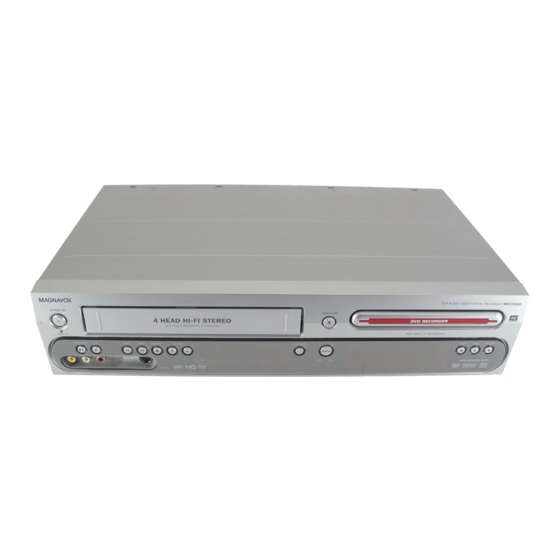
dvd recorder & video cassette recorder
Hide thumbs
Also See for DVDR600VR/37:
- Owner's manual (88 pages) ,
- Specifications (2 pages) ,
- Quick use manual (2 pages)
Table of Contents
Advertisement
Philips Consumer Electronics Company
A Division of Philips Electronics North America Corporation
Technical Service Data
Service Solutions Group
Technical Publications Dept.
P.O. Box 555, 401 E. Old Andrew Johnson Hwy.
Jefferson City,TN 37760
DVD Recorder &
Video Cassette Recorder
Service Manual
PHILIPS
Model: DVDR600VR/37
DVD Recorder & Video Cassette Recorder
First Issue: 9/04
©2004 Philips Consumer Electronics Company
Sec. 1A: Main Section
( DVDR600VR/37, MRV700VR/17 )
Specifications
Operating Instructions
Adjustment Procedures
Schematic Diagrams and CBA's
Exploded Views
Cabinet & Electrical Parts Lists
Sec. 2: Deck Mechanism Section
Sec. 3: DVD+RW Basic Engine
VAD8041 12NC: 3122 785 14850
For repair information on the Basic
Engine.
MAGNAVOX
Model: MRV700VR/17
MANUAL 5903
Advertisement
Chapters
Table of Contents

Related Manuals for Philips DVDR600VR/37


Summary of Contents for Philips DVDR600VR/37
-
Page 1: Dvd Recorder
Philips Consumer Electronics Company MANUAL 5903 A Division of Philips Electronics North America Corporation Sec. 1A: Main Section Technical Service Data ( DVDR600VR/37, MRV700VR/17 ) Service Solutions Group Specifications Technical Publications Dept. Operating Instructions P.O. Box 555, 401 E. Old Andrew Johnson Hwy. - Page 2 Philips Consumer Electronics Company MANUAL 5903 A Division of Philips Electronics North America Corporation Sec. 1A: Main Section Technical Service Data ( DVDR600VR/37, MRV700VR/17 ) Service Solutions Group Specifications Technical Publications Dept. Operating Instructions P.O. Box 555, 401 E. Old Andrew Johnson Hwy.
- Page 3 Proper service and repair is important to the safe, reliable operation of all Philips Consumer Electronics Company** Equipment. The service procedures recommended by Philips and described in this service manual are effective methods of performing service operations. Some of these service operations require the use of tools specially designed for the purpose.
-
Page 4: Table Of Contents
TABLE OF CONTENTS [ Main Section ] Page SPECIFICATIONS ................................. 1-1-1 IMPORTANT SAFETY PRECAUTIONS ..........................1-2-1 STANDARD NOTES FOR SERVICING ..........................1-3-1 FUNCTION INDICATOR SYMBOLS............................1-4-1 PREPARATION FOR SERVICING............................1-5-1 OPERATING CONTROLS AND FUNCTIONS ........................1-6-1 REMOTE CONTROL OPERATION ............................1-7-1 CABINET DISASSEMBLY INSTRUCTIONS ......................... -
Page 5: Specifications
SPECIFICATIONS < VCR Section > Description Unit Minimum Nominal Maximum Remark 1. Video 1-1. Video Output (PB) Vp-p SP Mode 1-2. Video Output (R/P) Vp-p 1-3. Video S/N Y (R/P) SP Mode 1-4. Video Color S/N AM (R/P) SP Mode 1-5. - Page 6 < DVD Section > ITEM CONDITIONS UNIT NOMINAL LIMIT 1. VIDEO 1-1. Video Output 75 ohm load Vp-p 1-2. S-Video Output Y (Luminance) 75 ohm load Vp-p C (Chrominance) 75 ohm load Vp-p 0.300 1-3. Component Output Y (Luminance) 75 ohm load Vp-p Pb (Chrominance) 75 ohm load...
-
Page 7: Important Safety Precautions
IMPORTANT SAFETY PRECAUTIONS Product Safety Notice I. Also check areas surrounding repaired locations. J. Be careful that foreign objects (screws, solder Some electrical and mechanical parts have special droplets, etc.) do not remain inside the set. safety-related characteristics which are often not evi- K. - Page 8 Safety Check after Servicing Examine the area surrounding the repaired location for damage or deterioration. Observe that screws, parts, Chassis or Secondary Conductor and wires have been returned to their original posi- tions. Afterwards, do the following tests and confirm the specified values to verify compliance with safety Primary Circuit Terminals standards.
-
Page 9: Standard Notes For Servicing
STANDARD NOTES FOR SERVICING Circuit Board Indications Pb (Lead) Free Solder When soldering, be sure to use the Pb free solder. 1. The output pin of the 3 pin Regulator ICs is indi- cated as shown. How to Remove / Install Flat Pack-IC Top View Bottom View 1. - Page 10 3. The flat pack-IC on the CBA is affixed with glue, so With Soldering Iron: be careful not to break or damage the foil of each (1) Using desoldering braid, remove the solder from all pin or the solder lands under the IC when removing pins of the flat pack-IC.
- Page 11 2. Installation With Iron Wire: (1) Using desoldering braid, remove the solder from all (1) Using desoldering braid, remove the solder from pins of the flat pack-IC. When you use solder flux the foil of each pin of the flat pack-IC on the CBA so which is applied to all pins of the flat pack-IC, you you can install a replacement flat pack-IC more can remove it easily.
- Page 12 Instructions for Handling Semi-conductors Electrostatic breakdown of the semi-conductors may occur due to a potential difference caused by electro- static charge during unpacking or repair work. 1. Ground for Human Body Be sure to wear a grounding band (1MΩ) that is prop- erly grounded to remove any static electricity that may be charged on the body.
-
Page 13: Function Indicator Symbols
FUNCTION INDICATOR SYMBOLS < VCR Section > Note: If a mechanical malfunction occurs, the power is turned off. When the power comes on again after that by pressing [STANDBY-ON] button, an error message is displayed on the TV screen for 5 seconds. Led Mode Indicator Active When reel or capstan mechanism is not functioning... - Page 14 < DVD Section > Note: If an error occurs, a message with the error number appears on the screen. X X Y Y Z Z Error code Nucleus nmber Nucleus group nmber Description Error No. Error Description Sends the device id and the module ids and revisions 010000 Getting the information succeeded.
- Page 15 Description Error No. Error Description 030400 Value read. 030401 Unable to initialise NVM. 030402 Reading the NVRAM contents failed. 030403 Length out of range. Read out one or more locations in the NVRAM. 030404 Unable to decode length. 030405 Offset out of range. 030406 Unable to decode offset.
- Page 16 Description Error No. Error Description 060300 Switching the clock output off succeeded. Switch the clock output off. 060301 Switching the clock output off failed. 060400 Selecting the input of the VIP succeeded. 060401 The user provided wrong input. Select an input video path to be switched to the analogue output of the VIP.
- Page 17 Description Error No. Error Description 090600 The command executed successfully. 090601 Sanyo drive init fails. 090602 Failed to close tray. 090603 Failed to get disc type. 090604 Not DVD+RW disc. Write data to and read data from a DVD+RW disc through the basic engine for verification of the writing.
- Page 18 Description Error No. Error Description 091200 Optimising jitter succeeded. 091201 There was a time-out while communicating. 091202 The Basic Engine returned an unexpected result. 091203 The Basic Engine returned an error code. This test measures the average jitter and bler values. A 091204 No acknowledge received from BE.
- Page 19 Description Error No. Error Description 092900 The command executed successfully. 092901 There was a time-out while communicating. 092902 The Basic Engine returned an unexpected result. Read the region code from the AV3. 092903 The BE returned an error code. 092904 No acknowledge received from BE.
- Page 20 Description Error No. Error Description Check the interface between the remote control and 100500 Remote Control test succeeded. the DCB by checking the key-code displayed. At least 100501 DCB could not be accessed by the analogue board. one key must be tested. The test can be exited by 100502 There was no response from the analogue board.
- Page 21 Description Error No. Error Description 110800 Reading the download-software version succeeded. The segment containing the download-software version could not be 110801 Get the software version of the download software of found. the analogue board. 110802 Communicating with the analogue board failed. 110803 The analogue board returned an unexpected result.
- Page 22 Description Error No. Error Description 111900 Storing the reference voltage for the tuner in NVRAM succeeded. 111901 Storing the reference voltage for the tuner in NVRAM failed. Store the reference voltage for the tuner in NVRAM. 111902 The user provided wrong input. 111903 Communicating with the analogue board failed.
- Page 23 Description Error No. Error Description 120900 Writing the data over IIC succeeded. 120901 No input specified. 120902 Invalid Bus ID number. 120903 No IIC address. 120904 Invalid IIC address. 120905 No number of bytes input. Perform an IIC write action on the digital board. 120906 Invalid number of bytes.
- Page 24 Description Error No. Error Description 122100 Turning off the virgin mode succeeded. 122101 Turning off VirginMode on the Analogue Board failed. Turn off the virgin mode functionality (e.g. the auto channel search upon startup). 122103 No DS errCode known for analogue board error: 122104 There was no response from the analogue board.
-
Page 25: Preparation For Servicing
PREPARATION FOR SERVICING How to Enter the Service Mode About Optical Sensors Caution: An optical sensor system is used for the Tape Start and End Sensors on this equipment. Carefully read and follow the instructions below. Otherwise the unit may operate erratically. What to do for preparation Insert a tape into the Deck Mechanism Assembly and press the PLAY button. -
Page 26: Operating Controls And Functions
OPERATING CONTROLS AND FUNCTIONS [ DVDR600VR/37 ] 1-6-1 E9480IB... - Page 27 1-6-2 E9480IB...
- Page 28 1-6-3 E9480IB...
- Page 29 [ MRV700VR/17 ] 1-6-4 E9480IB...
- Page 30 1-6-5 E9480IB...
- Page 31 1-6-6 E9480IB...
-
Page 32: Remote Control Operation
REMOTE CONTROL OPERATION [ DVDR600VR/37 ] 1-7-1 E9480IBR... - Page 33 1-7-2 E9480IBR...
- Page 34 [ MRV700VR/17 ] 1-7-3 E9480IBR...
- Page 35 1-7-4 E9480IBR...
-
Page 36: Cabinet Disassembly Instructions
CABINET DISASSEMBLY INSTRUCTIONS Comparison Chart of Models and Marks 2. Disassembly Method Model Mark REMOVAL DVDR600VR/37 REMOVE/*UNHOOK/ LOC. PART Fig. UNLOCK/RELEASE/ Note MRV700VR/17 UNPLUG/DESOLDER 1. Disassembly Flowchart Top Cover D1 6(S-1) This flowchart indicates the disassembly steps to gain access to item(s) to be serviced. When reassembling, *2(L-1), Tray Panel, follow the steps in reverse order. - Page 37 aligning the hole of Cam Gear with the pin of LD- REMOVAL SW, the shaft of Cam Gear with the hole of LD-SW REMOVE/*UNHOOK/ LOC. PART as shown in Fig. D8. Fig. UNLOCK/RELEASE/ Note UNPLUG/DESOLDER Deck (S-22), (S-23), [18] Assembly Desolder (S-1) (S-1)
- Page 38 (S-5) (S-12) [5] Jack-A CBA [9] FFC Friction Plate (S-13) (S-10) (S-6) (S-11) (S-12) [10] Rear [6] Jack-B CBA Panel Unit (S-12) Fig. D3 CN209 [7] DVD Mecha & FE Assembly (S-8) (S-7) CN210 Fig. D5 [14] Rear Panel Connector 1109 (S-9) (S-16) (S-15) [8] Digital...
- Page 39 (S-20) (S-19) (S-20) (S-19) (S-19) (S-20) CN214 (S-20) (S-20) [15] (S-21) (S-17) Front (S-17) [17] VCR Chassis (S-18) Unit [16] Bracket R Fig. D7 1-8-4 E9480DC...
- Page 40 Cylinder Assembly FE Head ACE Head Assembly [18] Deck Assembly SW202 LD-SW (S-24) [21] CPU CBA Unit (S-24) CN215 (S-24) [20] Main CBA CN216 (S-22) [18] Deck Assembly [20] Main Cam Gear Hole [19] Function Shaft (S-23) Hole LD-SW Desolder [20] Main CBA Lead with blue stripe...
- Page 41 (S-25) (S-25) [22] Deck Pedestal [23] Front Bracket R [ A ] (S-27) (S-26) iLink Cable Fig. D9 1-8-6 E9480DC...
- Page 42 HOW TO EJECT MANUALLY 1. Put tape on the Maintenance Tool. (Please use a metallic plate as shown below as a maintenance tool.) Maintenance Tool Size 50mm Tape 2. Insert the Maintenance Tool under the Tray Panel as shown. 3. Pull out and raise the Maintenance Tool up as shown to release two locking tabs of the Tray Panel. 4.
-
Page 43: How To Initialize The Dvd Recorder
HOW TO INITIALIZE THE DVD RECORDER To put the program back at the factory-default, initialize the DVD recorder using the following procedure. 1. Press and hold the [DVD STOP C] button on the DVD recorder. 2. Insert the AC plug to an AC outlet. 3. -
Page 44: Electrical Adjustment Instructions
ELECTRICAL ADJUSTMENT INSTRUCTIONS General Note: "CBA" is an abbreviation for "Circuit Board Assembly." NOTE: Figure 1 1.Electrical adjustments are required after replacing circuit components and certain mechanical parts. It is important to do these adjustments only after EXT. Syncronize Trigger Point all repairs and replacements have been com- pleted. -
Page 45: Adjustment Points And Test Points
Adjustment Points and Test Points Main CBA Top View TP751 V-OUT TP301 C-PB TP302 RF-SW VR201 SW-P TP513 CTL TP204 S-INH TEST POINT INFORMATION : Indicates a test point with a jumper wire across a hole in the PCB. TEST POINTS NOT USED IN ELECTRICAL ADJUSTMENTS Test Point Used in: Page No. -
Page 46: Firmware Renewal Mode
FIRMWARE RENEWAL MODE 1. Make a copy of the data for update to a CD-R or CD-RW. 2. Set the disc made in Step 1 on the tray and close. 3. Turn on the DVD recorder while pushing [DVD OPEN/CLOSE A] button and [DVD RECORD I] button at the same time. -
Page 47: Rework Procedure Ieee Unique Number
REWORK PROCEDURE IEEE UNIQUE NUMBER The procedure describes how to upgrade sets with a unique number after repair. This unique number is stored in the NVRAM of the FEBE board at the end of the production line. This procedure is only valid or necessary when: - The FEBE board is replaced - NVRAM on the FEBE board is replaced - NVRAM is cleared... -
Page 48: Block Diagrams
BLOCK DIAGRAMS Servo / System Control Block Diagram 1-11-1 E9480BLS... -
Page 49: Sub System Control Block Diagram
Sub System Control Block Diagram 1-11-2 E9480BLSUB... -
Page 50: Video Block Diagram
Video Block Diagram 1-11-3 E9480BLV... -
Page 51: Video Input/Output Select Block Diagram
Video Input/Output Select Block Diagram 1-11-4 E9480BLVIS... -
Page 52: Audio Block Diagram
Audio Block Diagram E9480BLA 1-11-5... -
Page 53: Audio Input/Output Select Block Diagram
Audio Input/Output Select Block Diagram 1-11-6 E9480BLAS... -
Page 54: Hi-Fi Audio Block Diagram
Hi-Fi Audio Block Diagram E9480BLH 1-11-7... -
Page 55: Power Supply Block Diagram
Power Supply Block Diagram 1-11-8 E9480BLP... -
Page 56: Schematic Diagrams / Cba's And Test Points
Under no circumstances should the original design be AREA B1 Line Number modified or altered without written permission from (1 to 3 digits) 1-D3 Philips Consumer Electronics Company. Philips assumes no liability, express or implied, arising out of any unauthorized modification of design. Servicer Examples: assumes all liability. -
Page 57: Main 1/7 Schematic Diagram Parts Location Guide
Main 1/7 Schematic Diagram Parts Location Guide < VCR Section > Ref No. Position Ref No. Position CAPACITORS RESISTORS C494 R499 C498 R500 C500 R502 C501 R505 C502 R512 C504 R513 C506 R514 C508 R517 C510 R518 C512 R521 C513 R522 C515 R523... -
Page 58: Main 1/7 Schematic Diagram
Main 1/7 Schematic Diagram < VCR Section > Voltage indications for PLAY, REC and DVD modes IC501 KEY VOLTAGE CHART on the Schematic Diagrams are as shown below: Pin No. KEY 1 (67 PIN) KEY 2 (66 PIN) Voltage PLAY MODE 0.00 ~ 0.51V STANDBY OUTPUT... -
Page 59: Main 2/7, Sensor, Function & Jack-B Schematic Diagram
Main 2/7, Sensor, Function & Jack-B Schematic Diagram < VCR Section > Voltage indications for PLAY, REC and DVD modes on the Schematic Diagrams are as shown below: IC225 MATRIX CHART PLAY MODE “ “ = SMD REC MODE (2.5) DVD MODE <... -
Page 60: Main 3/7 Schematic Diagram
Main 3/7 Schematic Diagram < VCR Section > Voltage indications for PLAY, REC and DVD modes on the Schematic Diagrams are as shown below: “ “ = SMD PLAY MODE REC MODE (2.5) DVD MODE < > THE SAME VOLTAGE FOR INDICATES THAT THE VOLTAGE PLAY,REC &... -
Page 61: Main 4/7 Schematic Diagram
Main 4/7 Schematic Diagram < VCR Section > Voltage indications for PLAY, REC and DVD modes on the Schematic Diagrams are as shown below: PLAY MODE “ “ = SMD REC MODE (2.5) DVD MODE < > THE SAME VOLTAGE FOR INDICATES THAT THE VOLTAGE PLAY,REC &... -
Page 62: Main 4/7 Schematic Diagram Parts Location Guide
Main 4/7 Schematic Diagram Parts Location Guide < VCR Section > Ref No. Position Ref No. Position CAPACITORS CAPACITORS C363 C407 C364 C410 C366 C368 IC226 C371 COILS C373 L214 C374 RESISTORS C375 C376 JC102 C377 R423 C379 R424 C380 R425 C381 R426... -
Page 63: Main 5/7 Schematic Diagram Parts Location Guide
Main 5/7 Schematic Diagram Parts Location Guide < VCR Section > Ref No. Position Ref No. Position Ref No. Position Ref No. Position Ref No. Position CAPACITORS CAPACITORS COILS RESISTORS RESISTORS C201 C345 L206 R294 R376 AA-3 C202 C346 L207 AA-3 R296 R377... -
Page 64: Main 5/7 Schematic Diagram
Voltage indications for PLAY, REC and DVD modes Main 5/7 Schematic Diagram < VCR Section > on the Schematic Diagrams are as shown below: PLAY MODE REC MODE (2.5) “ “ = SMD DVD MODE < > THE SAME VOLTAGE FOR INDICATES THAT THE VOLTAGE PLAY,REC &... -
Page 65: Main 6/7 Schematic Diagram
Voltage indications for PLAY, REC and DVD modes Main 6/7 Schematic Diagram < VCR Section > on the Schematic Diagrams are as shown below: PLAY MODE “ “ = SMD REC MODE (2.5) DVD MODE < > THE SAME VOLTAGE FOR INDICATES THAT THE VOLTAGE PLAY,REC &... -
Page 66: Main 6/7 Schematic Diagram Parts Location Guide
Main 6/7 Schematic Diagram Parts Location Guide < VCR Section > Ref No. Position Ref No. Position Ref No. Position Ref No. Position CAPACITORS CAPACITORS RESISTORS RESISTORS C204 EE-4 C355 EE-1 DD-2 R244 FF-1 C205 EE-4 C356 FF-3 JC05 HH-1 R246 FF-1 C206... -
Page 67: Main 7/7 Schematic Diagram Parts Location Guide
Main 7/7 Schematic Diagram Parts Location Guide < VCR Section > Ref No. Position Ref No. Position Ref No. Position CAPACITORS RESISTORS C554 NN-3 IC230 MM-1 R607 KK-3 C561 NN-1 IC231 KK-3 R608 KK-3 C563 MM-3 IC232 LL-3 R609 LL-1 C565 MM-4 IC233... -
Page 68: Main 7/7 & Dvd Open/Close Schematic Diagram
Main 7/7 & DVD Open/Close Schematic Diagram < VCR Section > Voltage indications for PLAY, REC and DVD modes on the Schematic Diagrams are as shown below: PLAY MODE “ “ = SMD REC MODE (2.5) DVD MODE < > THE SAME VOLTAGE FOR INDICATES THAT THE VOLTAGE PLAY,REC &... - Page 69 < VCR Section > Main CBA Parts Location Guide Ref No. Position Ref No. Position Ref No. Position Ref No. Position Ref No. Position Ref No. Position Ref No. Position Ref No. Position Ref No. Position Ref No. Position Ref No. Position CAPACITORS CAPACITORS...
-
Page 70: Main Cba Top View
Main CBA Top View < VCR Section > Sensor CBA Top View < VCR Section > TP751 TO SENSOR CBA V-OUT (START-SENSOR) BHB300F01014A BHB300F01014B TO SENSOR CBA (END-SENSOR) TP301 C-PB TP302 RF-SW VR201 SW-P TP513 TP204 S-INH BE9480F01011A 1-12-23 1-12-24... -
Page 71: Main Cba Bottom View
Main CBA Bottom View < VCR Section > PIN 5 OF PIN 7 OF PIN9 OF PIN18 OF PIN 1 OF CN213 CN213 CN213 CN213 CN213 PIN 29 OF CN215 WF10 PIN 2 OF CN211 BE9480F01011A 1-12-25 1-12-26... -
Page 72: Function Cba Top/Bottom View
Function CBA Bottom View Function CBA Top View < VCR Section > < VCR Section > FUNCTION CBA PARTS LOCATION GUIDE Ref No. Position DIODES D951 D952 RESISTORS R951 R952 R953 SWITCHES SW951 SW952 BE9480F01011B JACK-B CBA PARTS LOCATION GUIDE Ref No. -
Page 73: Front Schematic Diagram
Front Schematic Diagram < VCR Section > FIP801 MATRIX CHART Voltage indications for PLAY, REC and DVD modes on the Schematic Diagrams are as shown below: 2j, 2p 2j, 2p 2j, 2p 2j, 2p 2j, 2p 2j, 2p 2j, 2p PLAY MODE “... -
Page 74: Front Cba Top/Bottom View
Front CBA Top View < VCR Section > Front CBA Bottom View < VCR Section > FRONT CBA PARTS LOCATION GUIDE Ref No. Position Ref No. Position Ref No. Position Ref No. Position Ref No. Position Ref No. Position Ref No. Position Ref No. -
Page 75: Jack-A Schematic Diagram
Jack-A Schematic Diagram < VCR Section > Power Supply Schematic Diagram Parts Location Guide < VCR Section > Ref No. Position Ref No. Position Ref No. Position JACK-A SCHEMATIC DIAGRAM CAPACITORS DIODES RESISTORS PARTS LOCATION GUIDE C1001 D1012 R1004 Ref No. Position Ref No. -
Page 76: Power Supply Schematic Diagram
Power Supply Schematic Diagram < VCR Section > CAUTION CAUTION ! Voltage indications for PLAY, REC and DVD modes FOR CONTINUED PROTECTION AGAINST FIRE HAZARD, Fixed voltage ( or Auto voltage selectable ) power supply circuit is used in this unit. on the Schematic Diagrams are as shown below: “... -
Page 77: Power Supply Cba Top View
Power Supply CBA Top View < VCR Section > CAUTION FOR CONTINUED PROTECTION AGAINST FIRE HAZARD, CAUTION ! REPLACE ONLY WITH THE SAME TYPE FUSE. Fixed voltage ( or Auto voltage selectable ) power supply circuit is used in this unit. ATTENTION : POUR UNE PROTECTION CONTINUE LES RISQES If Main Fuse (F1001) is blown, check to see that all components in the power supply D'INCELE N'UTILISER QUE DES FUSIBLE DE MÊME TYPE. -
Page 78: Power Supply Cba Bottom View
Power Supply CBA Bottom View < VCR Section > CAUTION ! CAUTION BECAUSE A HOT CHASSIS GROUND IS PRESENT IN THE POWER Fixed voltage ( or Auto voltage selectable ) power supply circuit is used in this unit. FOR CONTINUED PROTECTION AGAINST FIRE HAZARD, SUPPLY CIRCUIT , AN ISOLATION TRANSFORMER MUST BE USED. -
Page 79: Cpu 1/2 Schematic Diagram
CPU 1/2 Schematic Diagram < DVD Section > Voltage indications for PLAY and STOP modes on the Schematic Diagrams are as shown below: “ “ = SMD PLAY MODE STOP MODE (2.5) THE SAME VOLTAGE FOR INDICATES THAT THE VOLTAGE BOTH PLAY &... -
Page 80: Cpu 2/2 Schematic Diagram
Voltage indications for PLAY and STOP modes CPU 2/2 Schematic Diagram < DVD Section > on the Schematic Diagrams are as shown below: PLAY MODE STOP MODE “ “ = SMD (2.5) THE SAME VOLTAGE FOR INDICATES THAT THE VOLTAGE BOTH PLAY &... -
Page 81: Digital Board Unit 1/10 Schematic Diagram
Digital Board Unit 1/10 Schematic Diagram < DVD Section > 1101 E1 1103 D12 1108 B8 1109 B12 2114 A10 RESET,UART,SERVICE,E_LINK 2116 F2 2117 G3 2118 G1 2119 C2 5103 +3V3D 2120 C11 BLM11 2121 D11 2122 G4 2123 H6 +3V3D 7127 2124 A12... -
Page 82: Digital Board Unit 2/10 Schematic Diagram
Digital Board Unit 2/10 Schematic Diagram < DVD Section > 1201 E2 1202 G5 1203 B2 2200 B3 IEEE1394 (DV) 2202 E3 2203 E2 2204 E2 2205 E3 2206 F2 2207 G2 +3V3_IEEE_A +3V3_IEEE_D +3V3_IEEE_PLL +3V3_IEEE_D +3V3_IEEE_D +3V3_IEEE_D 2208 G3 2209 G3 2210 H2 2211 H2... -
Page 83: Digital Board Unit 3/10 Schematic Diagram
Digital Board Unit 3/10 Schematic Diagram < DVD Section > 2301 H1 2302 H1 2303 H1 2304 H1 2305 H1 DVD RECORDER PROCESSOR 2306 H2 F317 2307 H2 3312 DMN_AGND SYS_RST# 2308 H2 2309 I2 3313 VIP_INTA 2310 I2 DMN_GPIO0 3314 2311 I2 2312 I1... -
Page 84: Digital Board Unit 4/10 Schematic Diagram
Digital Board Unit 4/10 Schematic Diagram < DVD Section > 2400 G4 3419-1 E10 2401 G5 3419-2 E10 2402 G5 3419-3 E10 2403 G5 3419-4 E10 TERMINATION AT DMN8600/DDR SDRAM 2404 G6 3420-1 E9 2405 G6 3420-2 E9 2406 H4 3420-3 E9 2407 H5 3420-4 F9... -
Page 85: Digital Board Unit 5/10 Schematic Diagram
Digital Board Unit 5/10 Schematic Diagram < DVD Section > 1500 C9 F524 D12 2501 H8 F525 C12 2502 C1 F526 E10 2503 C2 F528 D3 2504 E3 F530 C3 POWER SUPPLY/OSC 2505 G8 F531 B3 2506 B1 F534 C2 2509 A7 2510 G10 2511 G10... -
Page 86: Digital Board Unit 6/10 Schematic Diagram
Digital Board Unit 6/10 Schematic Diagram < DVD Section > 1102 F7 2601 A12 2602 A12 2603 A10 GPIOs /IDE GPIOs 2604 A6 +3V3_GPIO 2605 B14 2606 B2 +3V3_GPIO 2607 C3 2610 G2 2603 3600 4602 DMN_GPIO0 7603 3600 A9 +3V3_GPIO +3V3_GPIO 74ALVT16373DGG... -
Page 87: Digital Board Unit 7/10 Schematic Diagram
Digital Board Unit 7/10 Schematic Diagram < DVD Section > 2756 F11 2757 G12 2758 I1 2759 I2 MEMORY (SDRAM/FLASH)/EEPROM 2760 I2 +3V3_FLASH 2761 I2 5701 +3V3 2762 I2 BLM31 2763 I3 2764 I3 SSTL2_VDD SSTL2_VDD F708 2765 I3 7708 16V 10u 2766 I4 AM29LV641DL... -
Page 88: Digital Board Unit 8/10 Schematic Diagram
Digital Board Unit 8/10 Schematic Diagram < DVD Section > 1704 C9 5807 I12 1802 H14 5808 I14 1900 H13 5809 F6 1904 D13 5810 G6 AUDIO/VIDEO INPUT/OUTPUT 2800 A4 5811 I6 2801 A4 5812 I2 2802 A4 5813 I2 2803 A4 5814 H10 VIP_ANALOG_VIDEO_INPUT... -
Page 89: Digital Board Unit 9/10 Schematic Diagram
Digital Board Unit 9/10 Schematic Diagram < DVD Section > 1002 G12 F905 B8 1903 I3 F906 B1 2947 A5 F907 B4 2948 A5 F908 C5 5982 F901 VIPS 2949 A6 F909 C1 +3V3 BLM11 2950 A6 F910 D3 VDDA 2951 A6 F911 D7 F900... -
Page 90: Digital Board Unit 10/10 Schematic Diagram
Digital Board Unit 10/10 Schematic Diagram < DVD Section > 1000-1 G2 1000-2 G2 1001-1 G2 1001-2 G2 VIDEO ENCODER 2012 C3 2013 B8 2014 B10 2015 B8 2016 B9 2017 C11 2018 C2 2019 C3 2021 C2 2022 C11 2023 E7 2024 E6 +2V5D_V... -
Page 91: Digital Board Unit Top View
Digital Board Unit Top View < DVD Section > 1-12-65 1-12-66... -
Page 92: Digital Board Unit Bottom View
Digital Board Unit Bottom View < DVD Section > 1-12-67 1-12-68... -
Page 93: Digital Board Unit Test Point View
Digital Board Unit Test Point View < DVD Section > 1-12-69 1-12-70... -
Page 94: Waveforms
WAVEFORMS NOTE: Input: COLOR BAR SIGNAL (WITH 1KHz AUDIO SIGNAL) TP751 Pin 7 of CN213 Pin 29 of CN215 V-OUT E-E 10 µ s 50mV x 10 VIDEO-C 0.2V 20µs A-OUT(L) 0.1µs TP751 UPPER Pin 2 of CN211 Pin 18 of CN213 TP302 WF10 LOWER... -
Page 95: Wiring Diagram
WIRING DIAGRAM 1-14-1 E9480WI... -
Page 96: System Control Timing Charts
SYSTEM CONTROL TIMING CHARTS [ VCR Section ] Mode SW : LD-SW LD-SW Position detection A/D Input voltage Limit Symbol (Calculated voltage) 3.76V~4.50V (4.12V) 4.51V~5.00V (5.00V) 0.00V~0.25V (0.00V) 1.06V~1.50V (1.21V) 0.66V~1.05V (0.91V) 1.99V~2.60V (2.17V) 1.51V~1.98V (1.80V) 3.20V~3.75V (3.40V) 0.26V~0.65V (0.44V) 4.51V~5.00V (5.00V) 2.61V~3.19V... - Page 97 Still/Slow Control Frame Advance Timing Chart 1) SP Mode 18 RF-SW The first rise of RF-SW after a rise in F-AD signal F-AD (Internal Signal) "H" "H" "Z" C-DRIVE "L" "L" Stop detection (T2) Acceleration Detection (T1) Slow Tracking Value PB CTL Reversal Limit Value 20ms...
- Page 98 2) LP/SLP Mode 18 RF-SW The first rise of RF-SW after a rise in F-AD signal F-AD (Internal Signal) "H" "H" "Z" C-DRIVE "L" "L" Stop detection (T2) Acceleration Detection (T1) Slow Tracking Value PB CTL Reversal Limit Value 20ms 27 C-F/R 79 H-A-SW 78 C-ROTA...
- Page 99 EJECT ST-S/ END-S "OFF" CASS.LOAD LD-FWD 0.2S LD-REV 0.7S LD-FWD 0.4S LD-FWD 0.2S LD-REV 0.2S LD-FWD 0.5S LD-REV STOP(A) PLAY LD-FWD PLAY LD-FWD LD-REV 0.2S LD-FWD PLAY PLAY PAUSE (SLOW) LD-FWD STILL(SLOW) PLAY LD-REV 0.2S LD-FWD PLAY STOP /EJECT LD-REV STOP(A) Fig.
- Page 100 STOP(A) STOP LD-REV 0.2S LD-FWD STOP /EJECT 1.0S LD-FWD 0.5S LD-REV STOP(A) LD-REV 0.2S LD-FWD STOP /EJECT LD-REV 1.0S LD-FWD 0.5S LD-REV STOP(A) LD-FWD PAUSE LD-FWD 2.5S Short REV LD-REV 0.2S LD-FWD REC PAUSE REC or PAUSE STOP /EJECT LD-FWD 1.5S LD-REV 0.2S...
- Page 101 [ DVD Section ] Tray in 5.0V Tray in 5.0V Tray out Sled Drive 1.35V Disc Drive 1.35V 1.35V Focus Drive 1.35V Tracking Drive Tray out 5.0V Tray in 5.0V Tray out 1.35V Sled Drive 1.35V Disc Drive 1.35V Focus Drive 1.35V Tracking Drive 1-15-6...
- Page 102 Spin up 5.0V Tray in 5.0V Tray out Sled Drive 1.35V Disc Drive 1.35V 1.35V Focus Drive 1.35V Tracking Drive Playing 5.0V Tray in 5.0V Tray out Sled Drive 1.35V Disc Drive 1.35V 1.35V Focus Drive 1.35V Tracking Drive 1-15-7 E9480TI...
-
Page 103: Ic Pin Function Descriptions
IC PIN FUNCTION DESCRIPTIONS [ VCR Section ] Signal Active Function Name Level IC228 ( SYSTEM CONTROL MICROPROCESOR ) System Reset Signal IN RESET (Reset=”L”) “H” ≥ 4.5V, “L” ≤ 1.0V 21 OUT LM-FWD/ Loading Motor FWD/ H/Z/L Signal Active REV Output Function Name... - Page 104 Signal Active Signal Active Function Function Name Level Name Level Drum PG/FG Input N.U. Not Used IN D-PFG PULSE Signal N.U. Not Used On/Off Switching IN ON/OFF N.U. Not Used Signal Color Phase Rotary Capstan Motor 78 OUT C-ROTA Changeover Signal IN C-FG Rotation Detection PULSE...
- Page 105 IC801 ( FRONT PANEL CONTROL ) Signal Name Function Name Signal Name Function N.U. Not Used Name N.U. Not Used N.U. Not Used N.U. Not Used N.U. Not Used Key Data 1 Input N.U. Not Used Key Data 2 Input N.U.
- Page 106 [ DVD Section ] Signal Name Function Name IC221 ( FIP DRIVER ) Signal Name Function Name Clock Input Serial Interface Strobe N.U. Not Used N.U. Not Used Power Supply VFT Output (Middle Electricity Output) Segment Output Pull Down Level OUT S9 Segment Output Indicator Panel Drive...
-
Page 107: Lead Identifications
LEAD IDENTIFICATIONS 2SA1175(J,H,F) KIA431A-AT 2SA1015-GR(TPE2) BC327-25 2SC2785(K) TL431A-TA 2SC1815-BL(TPE2) BC337-25-AT BN1F4M-T 2SC1815-GR(TPE2) BC546-B-AT KRA103M 2SC2120-Y(TPE2) BC547-B-AT KRC108M KTC3198(GR,Y) BC547-S-BB KTA1266(GR) KTC3203(Y) BC557-B-AT KTA1267(GR,Y) KTC3193(Y) KTC3199(BL,Y) 1 2 3 E C B E C B C B E PT6313-S-TP MC33078DR2 2SK2095N 2SC536NF-NPA-AT 2SK3563 BU4052BCF-E2... -
Page 108: Electrical Parts List
4835 122 87639 ±10% (B) ● C218 CHIP CERAMIC CAP .(1608) 1µF/10V CHD1AK30B105 4835 122 87639 To order parts call the TOLL FREE Philips Sales ±10% (B) ● C219 CHIP CERAMIC CAP .(1608) 1µF/10V CHD1AK30B105 4835 122 87639 Center number: 1 - 800 - 851 - 8885 ±10% (B) - Page 109 Ref. No. Description ID No. Part No. Ref. No. Description ID No. Part No. ● ● C256 CHIP CERAMIC CAP .(MELF) 470pF/50V CZM1JK30B471 4835 122 87203 C323 CHIP CERAMIC CAP .(1608) 0.1µF/25V CHD1EK30B104 4835 122 87213 ±10% (W) ±10% (B) or C258 ELECTROLYTIC CAP .
- Page 110 Ref. No. Description ID No. Part No. Ref. No. Description ID No. Part No. C364 ELECTROLYTIC CAP . 4.7µF/25V ±20% CE1EMAVSL4R7 4835 124 47407 CHIP CERAMIC CAP .(1608) 0.1µF/25V CHD1EZ30F104 4835 122 87213 +80/-20% (F) or C366 ELECTROLYTIC CAP . 0.1µF/50V ±20% CE1JMAVSLR10 4835 124 47048 CHIP CERAMIC CAP .
- Page 111 Ref. No. Description ID No. Part No. Ref. No. Description ID No. Part No. ● C477 ELECTROLYTIC CAP . 10µF/16V ±20% CE1CMAVSL100 4835 124 47268 C538 CHIP CERAMIC CAP .(MELF) 0.01µF/16V CZM1CZ30F103 4835 122 87647 +80/-20% (F) ● C478 CHIP CERAMIC CAP .(1608) 2700pF/50V CHD1JK30B272 4835 122 87098 C543...
- Page 112 Ref. No. Description ID No. Part No. Ref. No. Description ID No. Part No. ● C602 CHIP CERAMIC CAP .(1608) 1000pF/50V CHD1JK30B102 4835 122 87153 CN211 FFC/FPC CONNECTOR, 22P 00-6232- JC62G22TM010 ---- --- ----- ±10% (B) 022-006-800 or ● C603 CHIP CERAMIC CAP .(1608) 0.1µF/25V CHD1EK30B104 4835 122 87213...
- Page 113 Ref. No. Description ID No. Part No. Ref. No. Description ID No. Part No. D238 ZENER DIODE DZ-6.8BSCT265 or NDTC0DZ6R8BS 4835 130 38027 CHOKE COIL 47µH-K LLBD00PKT001 4835 157 58208 ZENER DIODE MTZJT-776.8C QDTC0MTZJ6R8 4835 130 37881 L226 PCB JUMPER D0.6-P5.0 JW5.0T ---- --- ----- D239...
- Page 114 Ref. No. Description ID No. Part No. Ref. No. Description ID No. Part No. CHIP RES.(1608) 1/10W 22k Ω ±5% ● +9V SWITCHING KTC3198(GR) "NPN" or NQS40KTC3198 4835 130 47946 R264 RRXAJR5Z0223 4835 111 37441 CHIP RES.(1608) 1/10W 82k Ω ±5% ●...
- Page 115 Ref. No. Description ID No. Part No. Ref. No. Description ID No. Part No. CHIP RES.(1608) 1/10W 150 Ω ±5% CHIP RES.(1608) 1/10W 6.8k Ω ±5% ● ● R370 RRXAJR5Z0151 4835 111 37334 R479 RRXAJR5Z0682 4835 111 37272 CHIP RES.(1608) 1/10W 10k Ω ±5% CHIP RES.(1608) 1/10W 8.2k Ω...
- Page 116 Ref. No. Description ID No. Part No. Ref. No. Description ID No. Part No. CHIP RES.(1608) 1/10W 10k Ω ±5% CARBON RES. 1/6W 470 Ω ±5% or ● R569 RRXAJR5Z0103 4835 111 37216 R626 RCX6JATZ0471 4835 111 37193 CHIP RES.(1608) 1/10W 10k Ω ±5% CARBON RES.
- Page 117 Ref. No. Description ID No. Part No. Ref. No. Description ID No. Part No. CHIP RES.(1608) 1/10W 150 Ω ±5% ● J373 CERAMIC CAP .(AX) 1000pF/50V ±10% CCA1JKT0B102 4835 122 47004 R952 RRXAJR5Z0151 4835 111 37334 CHIP RES.(1608) 1/10W 150 Ω ±5% ●...
- Page 118 Ref. No. Description ID No. Part No. Ref. No. Description ID No. Part No. # METALLIZED FILM CAP . 0.068µF/275V CT2E683DC015 4835 121 47725 # IC, ERROR VOLTAGE DET EL817A or NPEA000EL817 9965 000 19672 ±10% # IC, ERROR VOLTAGE DET EL817B or NPEB000EL817 4835 209 47615 C1016...
- Page 119 Ref. No. Description ID No. Part No. Ref. No. Description ID No. Part No. CARBON RES. 1/4W 680k Ω ±5% R1023 RCX4JATZ0684 4835 110 57227 C805 ELECTROLYTIC CAP . 22µF/25V ±20% CE1EMAVSL220 9965 000 25518 R1024 SWITCHING DIODE 1N4148M or NDTZ01N4148M 4835 130 37048 C806...
- Page 120 Ref. No. Description ID No. Part No. Ref. No. Description ID No. Part No. Q803 SWITCHING BC547-S-BB NQSB000BC547 9965 000 25523 FMN CONNECTOR, TOP 8P 08FMN- JCFNG08JG002 ---- --- ----- BTRK Q805 INVERTER BC547-S-BB NQSB000BC547 9965 000 25523 DIODE Q806 DRIVE BC547-S-BB NQSB000BC547 9965 000 25523...
- Page 121 Ref. No. Description ID No. Part No. SW905 TACT SWITCH KSM0614B SST0101HH013 4835 276 17282 SW905 TACT SWITCH SKQSAF001A SST0101AL041 4835 276 17282 SW905 TACT SWITCH TC-1104(H=9.5) SST0101DNG01 4835 276 17356 MISCELLANEOUS JK901 S TYPE JACK MDC1-03D-002 JXEJ040RP001 9965 000 25533 20040914 1-18-14 E9480EL...
-
Page 122: Exploded Views
EXPLODED VIEWS Cabinet 2L011 2L071 Comparison Chart of 2L011 2L071 2L071 Models and Marks 2L071 AC1001 2L081 Model Mark 2L082 2L011 DVDR600VR/37 2L062 MRV700VR/17 2L044 2L100 2B33 2L081 W009 2L044 FM1001 2B55 CPU CBA Unit 2L018 2L044 2B10 2B51 2L024... - Page 123 Packing [ A ] Unit (A27) PROTECT Comparison Chart of Models and Marks Model Mark DVDR600VR/37 MRV700VR/17 1-19-3 E9480PEX...
-
Page 124: Mechanical Parts List
(---- --- ----- or blank) are not normally available. 2B52 FIBER, HOLDER 1VM421013 ---- --- ----- 2B53 TAPE, HIMELON 0VM415649 ---- --- ----- To order parts call the TOLL FREE Philips Sales 2B54 RUBBER CUSHION(D) 1VM420881 ---- --- ----- 2B55 SIDE BOARD 1VM421021 ---- --- -----... - Page 125 Ref. No. # Mark Description ID No. Part No. TOP PAD 1VM420911 ---- --- ----- ACCESSORIES REMOTE CONTROL UNIT DUAL NA724UD 9965 000 25429 REMOCON REMOTE CONTROL UNIT DUAL NA510UD 4835 218 37367 REMOCON DRY BATTERY 2PACK R6-B500/01S XB0M142CZB01 RF CABLE 2.5C-2V WPZ0901TM002 4835 321 17157 ACCESSORY BAG 0VM415576...
- Page 126 Philips Consumer Electronics Company MANUAL 5897 A Division of Philips Electronics North America Corporation Technical Service Data Service Solutions Group Sec. 2: Deck Mechanism Section Technical Publications Dept. Standard Maintenance P.O. Box 555, 401 E. Old Andrew Johnson Hwy. Disassembly / Assembly of Mechanism...
- Page 127 Proper service and repair is important to the safe, reliable operation of all Philips Consumer Electronics Company** Equipment. The service procedures recommended by Philips and described in this service manual are effective methods of performing service operations. Some of these service operations require the use of tools specially designed for the purpose.
- Page 128 TABLE OF CONTENTS [ Deck Mechanism Section ] Page STANDARD MAINTENANCE ............. . . 2-1-1 SERVICE FIXTURE &...
- Page 129 STANDARD MAINTENANCE Service Schedule of Components H: Hours : Check I: Change Deck Periodic Service Schedule Ref.No. Part Name 1,000 H 2,000 H 3,000 H 4,000 H Cylinder Assembly Loading Motor Assembly Pulley Assembly B587 Tension Lever Assembly ACE Head Assembly B573, B574 Reel (SP)(D2), Reel (TU)(D2) Capstan Motor...
- Page 130 Cleaning Cleaning of ACE Head Clean the head with a cotton swab. Cleaning of Video Head Procedure Clean the head with a head cleaning stick or chamois 1.Remove the top cabinet. cloth. 2.Dip the cotton swab in 90% isopropyl alcohol and Procedure clean the ACE Head.
-
Page 131: Service Fixture And Tools
SERVICE FIXTURE AND TOOLS 4835 310 57025 4835 310 57043 Flat Screw Driver VFMS0001H6 Back Tension Meter (Purchase Locally) Alignment Tape (Made in USA) 4835 310 57027 Metric Thickness Gauges Lock Screw Driver Post Adjustment Screwdriver (Purchase Locally) (Purchase Locally) 4835 310 57034 Head Cleaning Stick 2-2-1... -
Page 132: Service Information
MECHANICAL ALIGNMENT PROCEDURES Explanation of alignment for the tape to correctly run B. Method to place the Cassette Holder in the tape- starts on the next page. Refer to the information below loaded position without a cassette tape on this page if a tape gets stuck, for example, in the 1. - Page 133 1. Tape Interchangeability Alignment Note: To do these alignment procedures, make sure that the Tracking Control Circuit is set to the preset position every time a tape is loaded or unloaded. (Refer to page 2-3-4, procedure 1-C, step 2.) Equipment required: Dual Trace Oscilloscope VHS Alignment Tape (VFMS0001H6) Guide Roller Adj.
- Page 134 1-A. Preliminary/Final Checking and 3. Check to see that the tape runs without creasing at Alignment of Tape Path Take-up Guide Post [4] or without snaking between Guide Roller [3] and ACE Head. (Fig. M3 and M5) Purpose: 4. If creasing or snaking is apparent, adjust the Tilt To make sure that the tape path is well stabilized.
- Page 135 5. To shift the CTL waveform, press CH UP or CH 4. If the envelope is as shown in Fig. M8, adjust the DOWN button on the remote control unit. Then height of Guide Roller [3] (Refer to Fig. M3) so that make sure that the maximum output position of PB the waveform looks like the one shown in Fig.
- Page 136 1-D. Azimuth Alignment of Audio/Con- trol/ Erase Head Purpose: To correct the Azimuth alignment so that the Audio/ Control/Erase Head meets tape tracks properly. Symptom of Misalignment: If the position of the Audio/Control/Erase Head is not properly aligned, the Audio S/N Ratio or Frequency Response will be poor.
- Page 137 DISASSEMBLY/ASSEMBLY PROCEDURES OF DECK MECHANISM Before following the procedures described below, be sure to remove the deck assembly from the cabinet. (Refer to CABINET DISASSEMBLY INSTRUCTIONS of Main Section.) All the following procedures, including those for adjustment and replacement of parts, should be done in Eject mode;...
- Page 138 REMOVAL INSTALLATION STEP START- REMOVE/*UNHOOK/ /LOC. PART ADJUSTMENT Fig. No. UNLOCK/RELEASE/ CONDITION UNPLUG/DESOLDER Cam Holder(F) --- [ A ] [22] [22] Cam Holder Assembly --- DM2, DM12 *(L-6) [ B,C,D,E,F,G,H,I,J,K ] [23] [23] Cam Gear (B) DM2, DM12 (C-2), *(P-5) [24] [24] Mode Gear...
- Page 139 Top View [41] [42] [43] [46] [14] [13] [11] [15] [36] [10] [12] [35] [34] [40] [29] [30] [16] [39] [38] Fig. DM1 Bottom View [20] [33] [32] [24] [26] [27] [25] [23] [28] [22] [21] [31] Fig. DM2 2-4-3 U29NDA_PC...
- Page 140 (S-1) (S-1) (L-1) (L-3) (L-2) (S-1A) (P-1) Installation of [3] and [6] First, insert [6] diagonally in [3] as shown below. Then, install [6] in [3] while pushing (L-1) in a direction of arrow. After installing [6] in [3], confirm that pin A of [3] enters hole A of [6] properly.
- Page 141 (S-4) [46] [47] (L-14) Desolder from bottom (S-3) Lead with White Stripe View for A Belt Fig. DM7 (S-2) [11] (S-4A) (L-4) (P-3) [13] Removal of [11] [12] 1) Remove screw (S-4A). 2) Unhook spring (P-2). [10] Lead with Desolder Release (L-4) while (P-2) Red Stripe...
- Page 142 Installation of [13] and [12] (S-5) [14] (S-6) [16] [13] [15] Hook spring (P-3) up to [12] and [13], then install then to (P-3) the specified position so that [12] will be floated slightly while holding [12] and [13]. (Refer to Fig. A.) [12] Fig.
- Page 143 (S-8) [22] (C-2) (C-1) [23] (L-6) [21] (P-5) [20] Cap Belt (P-5) [28] Installation position of Cap Belt [21] Cap Belt When installing [23], install the spring (P-5) to [28] as shown in the left figure, and then install [23] while Pin on pressing the spring (P-5) to bottom...
- Page 144 Installation of [25] [25] (C-4) Position of Mode Lever when installed Pin of [35] Pin of [31] Pin of [34] (S-9) (L-10) (L-8) (C-3) [27] [24] [28] Bottom View [26] [25] (L-9) [28] Align [25] and [28] as shown. First groove on [28] First tooth on [44] [28] When reassembling [28],...
- Page 145 [36] Break belt (P-7) [34] [40] (P-8) turn [37] (L-12) turn [38] (P-9) turn [ A,H,I,J,K ] [44] [45] Slide [39] [35] Fig. DM17 Fig. DM15 [42] [41] [43] (L-13) Fig. DM16 2-4-9 U29NDA_PC...
- Page 146 ALIGNMENT PROCEDURES OF MECHANISM The following procedures describe how to align the Alignment 1 individual gears and levers that make up the tape load- Loading Arm (SP) and (TU) Assembly ing/unloading mechanism. Since information about the state of the mechanism is provided to the System Install Loading Arm (SP) and (TU) Assembly so Control Circuit only through the Mode Switch, it is that their triangle marks point to each other as...
- Page 147 DECK EXPLODED VIEWS Deck Mechanism View 1 Mark Description Floil G-684G or Multemp MH-D (Blue grease) SLIDUS OIL #150 B494 L1467 L1191 B553 B411 B567 L1053 B410 L1051 Chassis Assembly Top View (Lubricating Point) B501 B560 L1450 L1450 B426 L1466 B121 B126 B492...
- Page 148 Deck Mechanism View 2 Mark Description Floil G-684G or Multemp MH-D (Blue grease) SLIDUS OIL #150 B587 B521 B487 SANKOUL FG84M (Yellow grease) B416 B591 B520 B590 B522 L1406 B148 B499 B508 B573 B574 B592 B558 B564 B557 B414 B565 B525 L1151 B417...
- Page 149 Deck Mechanism View 3 Mark Description Floil G-684G or Multemp MH-D (Blue grease) SLIDUS OIL #150 L1321 B347 L1321 B355 B354 Comparison Chart of Models and Marks Model Deck Part No. Mark MC132EMG/17 N2226FT MVR440MG/17 N2240FL MVR450MG/17 N2240FL MVR650MG/17 N2260FL DVP620VR/17 N2260FL B483...
- Page 150 4835 402 97875 E,F ,G B359 CLEANER LEVER MK10 0VM304413 4835 402 97845 To order parts call the TOLL FREE Philips Sales B360 CLEANER ROLLER MK9 0VM410032C 4835 464 57553 Center number: 1 - 800 - 851 - 8885 B361...
- Page 151 Ref. # Mark Pos. Description ID No. Part No. B571 P .S.W CUT 1.6X4.0X0.5T 0VM408485A ---- --- ----- B573 REEL(SP)(D2) MK12 0VM203755 4835 528 17057 B574 REEL(TU)(D2) MK12 0VM203756 4835 528 17058 B587 TENSION LEVER ASSEMBLY 0VSA13279 4835 464 57598 MK12 B590 BRAKE ARM(TU) MK12...
- Page 152 All rights reserved. No part of this publication may be reproduced, stored in a retrieval system or transmitted, in any form or by any means, electronic, mechanical, photocopying, or otherwise without the prior permission of Philips. Published by GH03 0495 Service PaCE...
-
Page 153: Technical Specifications
EN 2 VAD8041 Technical Specifications and Connection Facilities 1. Technical Specifications and Connection Facilities VAD8041 functionality: • Loading of 8 cm and 12 cm discs by a motorized tray • Disc type recognition and in case of a DVD+RW disc laser power calibration •... -
Page 154: Safety Instructions, Warnings And Notes
Safety Instructions, Warnings and Notes VAD8041 EN 3 2. Safety Instructions, Warnings and Notes Safety Instructions Warnings 2.1.1 General Safety 2.2.1 General Safety regulations require that during a repair: • All ICs and many other semiconductors are susceptible to electrostatic discharges (ESD, symbol ). Careless •... -
Page 155: Directions For Use(No Dfu Necessary)
EN 4 VAD8041 Directions For Use Directions For Use Not applicable... -
Page 156: Mechanical Instructions
Mechanical Instructions VAD8041 EN 5 4. Mechanical Instructions Note that exploded views can be found in chapter 10 General Follow the dismantling instructions in described order. Never touch the lens of the OPU. Take sufficient ESD measures during handling. Dismantling You can divide the Basic Engine into the following parts: 1. - Page 157 EN 6 VAD8041 Mechanical Instructions Tray – Remove encasing as as described in 4.3 – Disengage the two holders that fix the tray [1], see figure 4- 2, and pull out the tray [2] Figure 4-3 Remove PWB DVD-M Caution: Never try to align or repair the DVD-Module itself! Only the factory can do this properly.
- Page 158 Mechanical Instructions VAD8041 EN 7 Sledge Motor Assembly Caution: Never try to align or repair the DVD-Module itself! Only the factory can do this properly. Service engineers are only allowed to exchange the sledge motor assy. – Eject the tray. –...
-
Page 159: Service Modes, Error Codes And Fault Finding
EN 8 VAD8041 Service Modes, Error Codes and Fault Finding 5. Service Modes, Error Codes and Fault Finding General Please refer to the service manual of the recorder for a description of the complete Diagnostics Software. In this manual only drive specific error codes are explained. Self test A power on self-test is incorporated in the software of this drive. - Page 160 Service Modes, Error Codes and Fault Finding VAD8041 EN 9 Error Codes error error meaning code With DSW command 910 (Digital Board Chrysalis) the set 0x18 atip_timeout_error Atip information could not be software can retrieve an overview of all occurred engine errors. read 0x19 atip_notfound_error...
- Page 161 EN 10 VAD8041 Service Modes, Error Codes and Fault Finding error error meaning code 0x39 opc_power_calculation_er Error during OPC power calcula- tion (samples are wrong) 0x3A opc_test_zone_full_error OPC can’t be performed because test zone is full 0x3B opc_bad_jitter_measurem The jitter measurement during ent_error OPC samples readback failed 0x3C...
- Page 162 Service Modes, Error Codes and Fault Finding VAD8041 EN 11 Byte 1 - 9: cumulative errors of previous error occurences. Format of the BE error bytes. Every individual error has its own bit in the 9-byte structure as described in the drawing below: byte 1 FOCUS FOCUS...
- Page 163 EN 12 VAD8041 Service Modes, Error Codes and Fault Finding 5.3.2 Cumulative errors These errors are stored in EEPROM and are thus non-volatile showing the complete error history of the drive. Byte 1 - 9: cumulative errors of previous player / inquiry error occurences.
-
Page 164: Block Diagrams, Waveforms, Wiring Diagram
Block Diagrams, Waveforms, Wiring Diagram. VAD 8041 EN 13 6. Block Diagrams, Waveforms, Wiring Diagram. Block Diagram LOADER RFN3 / RFP3, IC7201 Pin 38/39 I417 FS diode OPU66 laser 650nm laser 780nm Actuator Temp. Sensor 650nm PD Disc Motor Sledge Stepper RADIAL Tray Switch... -
Page 165: Testpoints Overview
Block Diagrams, Waveforms, Wiring Diagram. VAD 8041 EN 14 Testpoints Overview TR 22005_001 070704... -
Page 166: Electrical Diagrams And Print-Layouts
Electrical Diagrams and Print-Layouts VAD 8041 EN 15 7. Electrical Diagrams and Print-Layouts Servo Board: OPU Interface 1100 A3 2100 C4 2101 H4 2102 E4 2103 A5 TO CHEETAH_QD/DRIVERS/CENTAURUS-DRAM-FLASHROM/DEBUG-AND-FLASH 2104 H3 2105 H4 2106 D9 2107 C7 {SERVO-MEAS,VREF,Vdel,Vthr,RW-Del,HIGH-GAIN,CD-MODE,VIG,VIE,VIA,VID,RFP,RFN,VIB,VIC,VIH,VIF,SERVO-COMM,FOC-,FOC+,RAD,IOthr,EFM-DATAP,EFM-DATAN,EFM-CLKP,EFM-CLKN,EFM_RWN,SCLK,SDIO,SEN,IoDel,WSB,SCL,SDA,HIGHPOWER,TEMP_SENSE} 2108 E7 2109 C7 2110 B7 3100 E5... -
Page 167: Servo Board: Cheetah (Diagram 2)
Electrical Diagrams and Print-Layouts VAD 8041 EN 16 Servo Board: Cheetah 2204 A4 2205 A5 2209 B2 2210 B2 2211 B3 2212 B3 2213 E7 2214 E7 {TIMOUT,RFP,RFN,VIA,VIB,VIC,VID,VIE,VIF,VIG,VIH,EFM-CLKP,EFM-CLKN,EFM-DATAP,EFM-DATAN,LASP,PPNO,RFP3,RFN3,RFREF,CALF,A1,A2,S2-XDN,D1_TILTN,D2_TLN,D3_REN,D4_FEN,S1_MIRN,MON1,MON2,SIDA,SICL,SILD,SDA,SCL,ALFA,FTC,RW-Del,EFM_RWN,RFP5,RFN5} 2215 E7 2217 E7 2218 E7 TO OPU/EPLD-LADIC-CON/LACONIC_IC/CENTAURUS 2219 B3 OPTIONB OPTIONB 2221 C4 2223 F7 2228 D7... -
Page 168: Servo Board: Laconic
Electrical Diagrams and Print-Layouts VAD 8041 EN 17 Servo Board: Laconic U1 E2 1302 D1 2300 B2 2301 B2 2302 B2 2303 D1 2304 D1 2305 F3 2306 B2 2307 B2 TO OPU/EPLD/CENTAURUS 2308 B5 2309 E6 2310 F4 {WSB,RW-Del,OSC_IN,PORN,SCL,SDA,SCLK,SDIO,SEN,HIGH-GAIN,CD-MODE,ALFA,LASP,Vdel,Vthr,VREF,IOthr,CD-MODE,HIGH-GAIN,IRQN,OSTR,SDA,SCL,IoDel} 2311 C1 2312 C2 5300... -
Page 169: Servo Board: Drivers
Electrical Diagrams and Print-Layouts VAD 8041 EN 18 Servo Board: Drivers (Overview) 1400 A3 I434 K5 1401 H1 I435 I3 2400 I7 I436 I3 2401 A12 I437 I3 2405 I7 I438 I4 2406 B12 I439 J7 TO CENTAURUS/DEBUG-AND-FLASH 2407 C8 I440 I7 2409 J7 I441 B13... - Page 170 Electrical Diagrams and Print-Layouts VAD 8041 EN 19 Servo Board: Drivers (Left page) 1400 I400 OUTSLD1+ I401 OUTSLD1- TOSTOCEN I402 OUTSLD2+ I408 OUTSLD2- SFW..R Top Contact D3V3 I406 I407 3406 TRAY-SW I432 Part 1 TRAYSW D3V3 I424 A: DC, 5 V/Div, 2us/Div TRAY-INOUT DRIVER-ON I472...
- Page 171 Electrical Diagrams and Print-Layouts VAD 8041 EN 20 Servo Board: Drivers (Right page) TO CENTAURUS/DEBUG-AND-FLASH 2421 OPU /CENTAURUS/POWER-CONN-AUDIO/DEBUG CONN 2401 OUTSLD1+ 100n FOC+ OUTSLD1- I403 3405 3404 1.65V TOSTOCEN 1.65V OUTSLD2+ I404 I405 S1V65 SERVO-COMM OUTSLD2- 2406 7401-1 I443 LM358D 1.65V I441 I442...
-
Page 172: Servo Board: Centaurus
Electrical Diagrams and Print-Layouts VAD 8041 EN 21 Servo Board: Centaurus (Overview) U2 A9 7500 B4 1500 A13 7502 F17 2500 B3 7503 K2 2501 B3 7504 E17 2502 B4 7505 K18 {AUXPW,TOSTOCEN,MRN,HIGHPOWER,RX2,OSC_IN,PORN,FO-,STEP-COS,STEP-SIN,FO+,SL,RA,FTC,S1_MIRN,D1_TILTN,D2_TLN,D3_REN,D4_FEN,OSTR,CALF,A2,A1,S2-XDN,TEMP_WARNING,EFM-DATAN,EFM-DATAP,EFM-CLKN,EFM-CLKP,PPNO,RFREF,RFP3,RFN3,T1,MOTO1,AUDIOL,AUDIOR,HRESET,HDASPN,CS1,CS0,HA2,HA0,HA1,HPDIAGN,HIRQ,HDACKN,IORDY,HRDN,HRWN,HDRQ,SDA,SCL,SILD,SICL,SIDA,RX2,TX2,TX1,RX1_MASTER,DRIVER-ON,MOTOR-ON,IRQN,TRAY-SW,TRAY-INOUT,VRIN,IEC958,EFM_RWN,RAD_MUTE,ACT_EMF,TEMP_SENSE} 2503 C2 7506 F20 2504 D2 I500 G17 3534 POWER-CONN-AUDIO/DEBUG AND FLASH/DRIVERS/CHEETAH_QD 2505 F2... - Page 173 Electrical Diagrams and Print-Layouts VAD 8041 EN 22 Servo Board: Centaurus Part1 {AUXPW,TOSTOCEN,MRN,HIGHRESET,HDASPN,CS1,CS0,HA2,HA0,HA1,HPDIAGN,HIRQ,HDACKN,IORDY,HRDN,HRWN,HDRQ,SDA,SCL,SILD,SICL,SIDA,RX2,TX2,TX1,RX1_MASTER,DRIVER-ON,MOTOR-ON,IRQN,TRAY-SW,TRAY-INOUT,VRIN,IEC958, I504 5501 5502 D1V8 D3V3 DEBUG(0:13) I512 7500 4502 PNX7850E A3V3 VSSA1 VDDA1 VSSA2 2503 VDDA2 I513 220n 3500 I503 MOTO1 VSSA3 VDDA3 RFN3 MOTO1 RFP3 3560 I507 RFREF HFIN_N...
- Page 174 Electrical Diagrams and Print-Layouts VAD 8041 EN 23 Servo Board: Centaurus Part 2 RFP3,RFN3,T1,MOTO1,AUDIOL,AUDIOR,HRESET,HDASPN,CS1,CS0,HA2,HA0,HA1,HPDIAGN,HIRQ,HDACKN,IORDY,HRDN,HRWN,HDRQ,SDA,SCL,SILD,SICL,SIDA,RX2,TX2,TX1,RX1_MASTER,DRIVER-ON,MOTOR-ON,IRQN,TRAY-SW,TRAY-INOUT,VRIN,IEC958,EFM_RWN,RAD_MUTE,ACT_EMF,TEMP_SENSE} 3534 POWER-CONN-AUDIO/DEBUG AND FLASH/DRIVERS/CHEETAH_QD 1500 CX-16F 16M93 2563 2564 A3V3 D3V3 5504 I509 2534 3581 100n 2538 OPTIONB I502 3591 3592 150R L501 L502 150R 3594 3595 150R 150R...
- Page 175 Electrical Diagrams and Print-Layouts VAD 8041 EN 24 Servo Board: Centaurus Part 3 CALF I520 2536 3509 I518 CALF UOPB I521 100n 2540 2507 UOPT 100n OSTR ALPHA0_STEPA0 I522 D1_TILTN 3510 D1_TILTN D2_TLN 3511 D2_TLN D3_REN 3512 D3_REN D4_FEN 3513 D4_FEN S1_MIRN 3579...
- Page 176 Electrical Diagrams and Print-Layouts VAD 8041 EN 25 Servo Board: Centaurus Part 4 6500 7502 I511 XDA(5) XDA5 I524 MAX6352SVUK-T OUTP 1 4503 PORN I541 PMLL414BL XDA(4) NC RESET XDA4 6503 6502 6501 CD GND I500 XDA(3) D3V3 XDA3 VCC5 BAS16 BAS16 BAS16...
-
Page 177: Servo Board: Power, Connectors (Diagram 6)
Electrical Diagrams and Print-Layouts VAD 8041 EN 26 Servo Board: Power, Connectors 1600-1 B12 3661 G2 I690 D4 1600-2 H12 3665 I9 I691 D5 I692 E5 1600-3 A12 3684 E11 1600-4 I12 3686 I3 I694 C2 4612 CENTAURUS-DRAM-FLASHROM 1600-5 A12 3689 C11 I695 I9 {AUDIOL,AUDIOR,RX1_MASTER,DEBUG(11),TX1,TX2,HDASPN,CS0,CS1,HA0,HA1,HA2,HPDIAGN,HIRQ,HDACKN,IORDY,HRDN,HRWN,HDRQ,HRESET,IEC958,RX2,RFP5,RFN5}... -
Page 178: Servo Board: Tray Motor Conn. (Diagram 7)
Electrical Diagrams and Print-Layouts VAD 8041 EN 27 Servo Board: Tray Motor Connections 0001 I7 0002 I8 1700 B1 1702 F5 1703 C6 OPU/CHEETAH_QD/DRIVERS/CENTAURUS/POWER-CONN 1705 E9 2700 I10 2701 I11 {RAD,SERVO-COMM,MOTO1,MRN,RX1_MASTER,TX1,A1,A2,CALF,VRIN,D1_TILTN,D2_TLN,D3_REN,D4_FEN,S1_MIRN,S2,FTC,MON1,MON2,RX2,TX2,PPNO,IRQN,PORN,T1,SCL,SDA,S2-XDN,DRIVER-ON,FO-,FO+,VFOO-,VFOO+,RA,VRAOO,SL+,SL-,FOC+,FOC-,TR+,TR-,TRAYSW,SL,VMOTO1O} 2702 I10 2703 I11 2704 I10 2705 I11 DEBUG(0:13) 2706 I10 2707 I11 3702 H5... - Page 179 Electrical Diagrams and Print-Layouts VAD 8041 EN 28 Layout Servo Board (Top Side) 1100 C4 3653 C1 2527 D2 2701 E3 3518 02 6500 D3 1600 C1 2528 D2 2702 B5 3519 C2 3665 A1 6501 D3 2100 C4 2529 C2 3520 C2 3684 C1 2703 D4...
- Page 180 Electrical Diagrams and Print-Layouts VAD 8041 EN 29 Layout Servo Board (Bottom Side) 1302 3456 6401 1400 3457 6402 1401 3458 6403 1500 3459 7107 1601 3460 7201 1602 3461 7300 1700 3462 7401 1702 3463 7402 1703 3464 7403 1705 3465 7405...
- Page 181 Electrical Diagrams and Print-Layouts VAD 8041 EN 30...
-
Page 182: Alignments (No Alignments Necessary)
Alignments, Test Procedures VAD8041 EN 31 8. Alignments, Test Procedures Adjust Laser Control In case no defect is found during the “Short Term Test Procedure” the test has to be extended with a burn in test - “Long Term Test Procedure”. In case of exchanging DVD-M or PWB an adjustment to align The burn in test described herein should be done with a OPU and PWB to each other is necessary. - Page 183 EN 32 VAD8041 Alignments, Test Procedures Flowchart for test instruction In the flowchart below it is described how and when the burn in test has to be carried out. incoming DVDR set for repair Remark 1: normal repair LVP 12.01: 7104 099 91731 track 28 -->...
- Page 184 Circuit Descriptions, Abbreviation List, and Data Sheets VAD8041 EN 33 9. Circuit Descriptions, Abbreviation List, and Data Sheets General Mechanically, the module consists of a motorized tray loader that contains the dual laser optical pickup unit and a PCBA that contains all the electronics needed to control the drive and The VAD8041 module, also known as “AV3.5”, is a Video interfacing to the MPEG encoder/decoder back-end...
- Page 185 EN 34 VAD8041 Circuit Descriptions, Abbreviation List, and Data Sheets • Paedic integrated photo detector with programmable gain pre-amplifier • Eeprom containing a number of values representing adjustments belonging to the OPU. The laser control and diode signal processor ICs together with an EEPROM are mounted on the OPU flex.
- Page 186 Circuit Descriptions, Abbreviation List, and Data Sheets VAD8041 EN 35 IC Servo Board IC7201, TZA1047: Servo Board, Analogue PReprocessor...
- Page 187 EN 36 VAD8041 Circuit Descriptions, Abbreviation List, and Data Sheets Table 1: Pin description Symbol Description Satellite segment H input GND1 Ground Central segment C input Central segment B input GND1 Ground RFNIN Inverse differential RF input / Single-ended RF read input RFPIN Differential RF input/ Single-ended RF write input...
- Page 188 Circuit Descriptions, Abbreviation List, and Data Sheets VAD8041 EN 37 Symbol Description GND2 Supply ground RF output voltage, positive RF output voltage, negative RFREF Reference voltage for differential RF output common mode level Output PP voltage CFTC FTC high pass filter capacitor FTC output GND1 Supply ground...
- Page 189 EN 38 VAD8041 Circuit Descriptions, Abbreviation List, and Data Sheets Symbol Description Single ended RF write input voltage VREF PDIC reference voltage output Satellite segment F input Only in EFM bypass mode EFM clock and data when not in EFM bypass mode.
- Page 190 Circuit Descriptions, Abbreviation List, and Data Sheets VAD8041 EN 39 IC7300, TZA1042: Servo Baord, Laser Power Controller Block diagram...
- Page 191 EN 40 VAD8041 Circuit Descriptions, Abbreviation List, and Data Sheets Pin description Symbol Type Drive Description /Thr. I hy Alpha Error Zero/Alpha Set Zero Digital Pad Supply DDD3 Digital Pad Supply SSD3 CLOCKOUT Buffered Oscillator Output OSCO Output of inverting Amplifier that forms oscillator OSCI Input of inverting Amplifier that forms oscillator TEST1D...
- Page 192 Circuit Descriptions, Abbreviation List, and Data Sheets VAD8041 EN 41 Pin description …continued Symbol Type Drive Description /Thr. IRQN Interrupt Request Not – active low interrupt request OSTR I hy OPC Strobe – request step in alpha setpoint / Board test input RESETN I hy...
- Page 193 EN 42 VAD8041 Circuit Descriptions, Abbreviation List, and Data Sheets IC7402, SSA56202: Servo Board, Motor Driver Fig. Block diagram.
- Page 194 Circuit Descriptions, Abbreviation List, and Data Sheets VAD8041 EN 43 PIN DESCRIPTION SYMBOL DESCRIPTION SYMBOL DESCRIPTION positive Hall input U COSC ext. capacitor for int. oscillator negative Hall input U i.c.2 internally connected positive Hall input V i.c.1 internally connected negative Hall input V INLD loading driver input...
- Page 195 EN 44 VAD8041 Circuit Descriptions, Abbreviation List, and Data Sheets IC7408,7409 BA5995: Servo Board, 4-channel BTL driver IC actuator and motor drive PreV PowV STAND BY (ch3 / 4) ch1 / 3 / 4 LEVEL SHIFT LEVEL SHIFT LEVEL SHIFT LEVEL SHIFT MUTE...
- Page 196 Circuit Descriptions, Abbreviation List, and Data Sheets VAD8041 EN 45 IC7500, PNX7850: Servo Board, Channel Codec/Buffer Manager/Servo Processor and Controller Nexperia PNX7850 conceptual block diagram SDRAM ANALOG CHANNEL CODEC BUFFER MANAGER SDRAM CD/DVD EFM WRITE CD/DVD CONTROLLER wobble WOBBLE CLOCK/DATA CHANNEL UDMA66 PROCESSOR...
- Page 197 Serial Clock I2C SCLK Audio serial bit clock Serial Data I2C SDRAM Synchronous DRAM Surface Mounted Components S/PDIF Sony Philips Digital InterFace SPIDRE Signal Processing Ic for Dvd REwritable SRAM Static Random Access Memory STBY STandBY SVCD Super Video CD...
- Page 198 Spareparts List VAD8041 EN 47 10. Spareparts List 10.1 Exploded Views Basic Engine TR 22001_001 300604...
- Page 199 EN 48 VAD8041 Spareparts List Loader * Height control for assemby of pos 120 + 121 AV3.5 Loader Assy_3139-197-60291-110 dd 2004-02-13 (POS)
- Page 200 Spareparts List VAD8041 EN 49 DVD-M TR 22003_001 300604...
- Page 201 EN 50 VAD8041 Spareparts List 2401 2238 586 59812 100nF 20-80% 50V 0603 2581 2238 586 59812 100nF 20-80% 50V 0603 Mechanical 2405 5322 126 11583 10nF 10% 50V 0603 2582 5322 126 11582 6.8nF 10% 63V 2406 2238 786 55648 82nF 10% 16V 0603 2583 5322 126 11582 6.8nF 10% 63V 2407...
- Page 202 Spareparts List VAD8041 EN 51 3216 4822 051 30759 75Ω 5% 0.062W 3504 4822 051 30472 4.7kΩ 5% 0.062W 3647 4822 051 30103 10kΩ 5% 0.062W 3217 4822 051 30333 33kΩ 5% 0.062W 3507 4822 051 30102 1kΩ 5% 0.062W 3648 2322 702 60829 82Ω...
- Page 203 EN 52 VAD8041 Spareparts List 5300 2422 549 44991 0603 EMI 100MHZ 600R 5301 2422 549 44991 0603 EMI 100MHZ 600R 5400 2422 536 00501 D62LCB 10µF PM20 5405 2422 549 44991 0603 EMI 100MHZ 600R 5406 2422 536 00501 D62LCB 10µF PM20 5501 2422 549 44991 0603 EMI 100MHZ 600R 5502...
- Page 204 Philips Consumer Electronics Company A Division of Philips Electronics North America Corporation Service Solutions Group Philips Consumer Electronics Company Service Solutions Group Technical Publications Dept. P.O. Box 555, 401 E. Old Andrew Johnson Hwy. Jefferson City,TN 37760...