mark_nctu
Advanced Member level 4
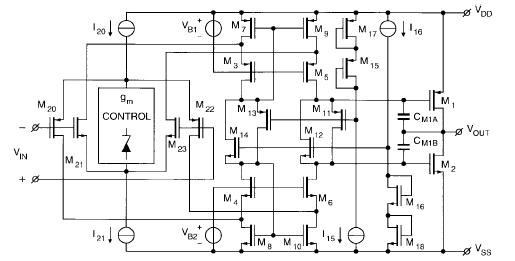
I design OPA with OTA + Class AB output.
When OPA at Vdd=5V , Phase has inverted to 180.
But low vdd (3V) is ok. Could some tell me how to
solve the problem?
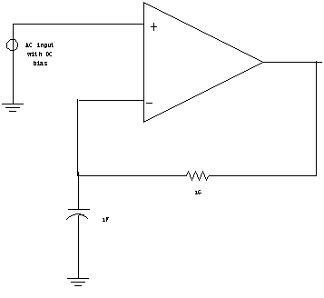
Circuit:
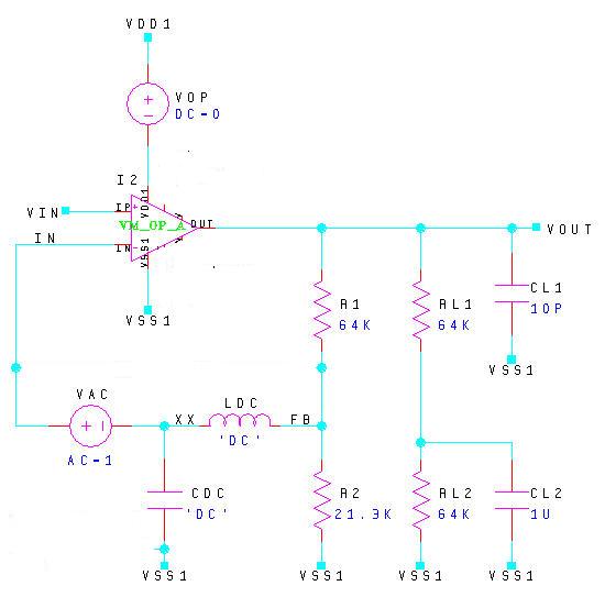
Test_Circuit:
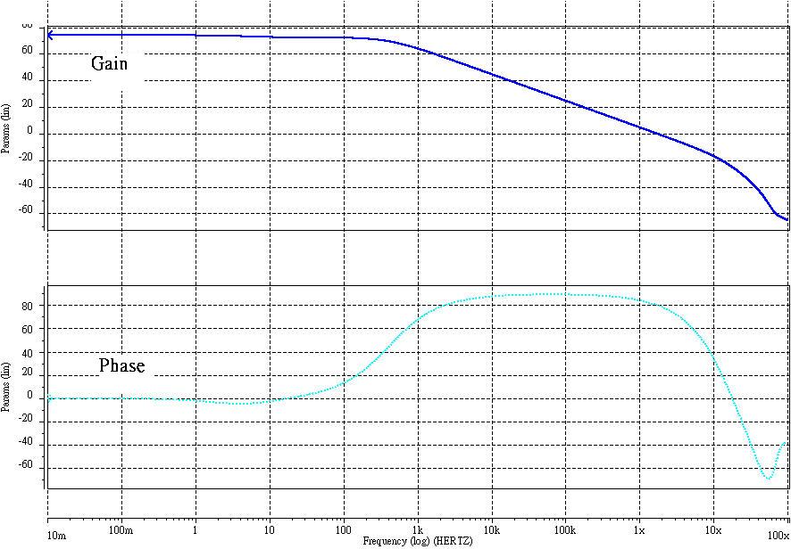
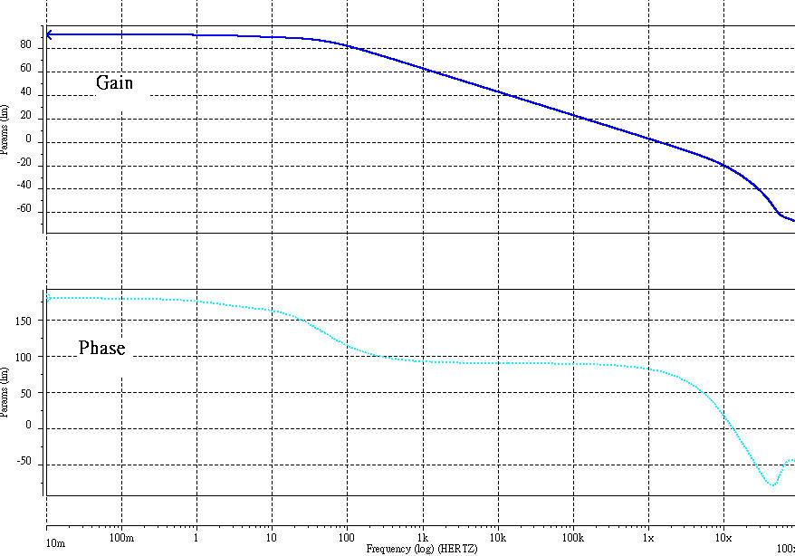
5V AC Result:
3V AC Result:
Added after 2 minutes:
Sorry Reupload 3V AC Result:
When OPA at Vdd=5V , Phase has inverted to 180.
But low vdd (3V) is ok. Could some tell me how to
solve the problem?
Circuit:
Test_Circuit:
5V AC Result:
3V AC Result:
Added after 2 minutes:
Sorry Reupload 3V AC Result: