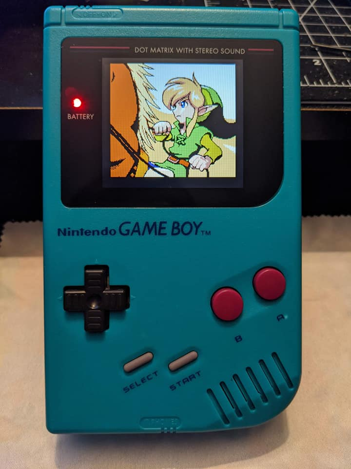
There’s just something about the original Game Boy that just is so aesthetically pleasing to me. But that old dim screen, gross! And the lack of Game Boy Color game support, so inconvenient! But you can just play them on a GBC, you say. But the GBC is so much smaller now compared to when I had one as a kid! My hands cramp up too quickly! It feels just a bit more chintzy than a nice, solid DMG! So in order to satiate my desire for a nicely lit, GBC-compatible DMG, I stuffed a GBA SP motherboard inside of a DMG case. It took a long time, got delayed more than once due to parts I didn’t have available, and was very frustrating at times, but I was able to finally complete it.
And after finishing my SP-in-a-DMG mod, I was really enjoying it… for about two weeks. It worked pretty well, but started showing some symptoms that something was not right. Sometimes the screen wouldn’t turn on. Only rarely, but it began occurring more and more often. Eventually, I was unable to boot at all, even without a game cartridge in the slot. After hours of troubleshooting, with some help from a few very knowledgeable folks on Discord (special thanks to gekkio for his help, and who has an infinite well of Game Boy knowledge on his website and github that I reference a lot), we determined the power management chip on the SP was bad. I guess that’s what I get for buying a cheap used SP on eBay that was labelled “for parts”. Unfortunately, the custom nature of the mod made replacing the SP board more trouble than I deemed it was worth. I declared the project dead, and stripped off most of the parts and threw the rest in a box to potentially tinker with in the future (but honestly, it will probably just stay in a box in my closet). Also taking it apart, I realized that some of the work was probably on the shoddier end, due in no part to trying to rush to finish it, and it being my first foray into Game Boy modding.
But! I was not deterred!
While completing my SP-based DMG, I was shown some actual completed GBC-in-DMG mods (henceforth called “DMG Color”) that I had not seen in my searching before starting the project. Putting the GBC inside the DMG case involves cutting off the bottom half of the board, underneath the cartridge connector. Luckily, even though I need to get rid of about 50% of the entire board, after doing some deep dives into the schematics and layout, I found out that the GBC is much easier to deal with than the SP is. The GBC is just a two-layer board, for starters, so knowing what I’m cutting is much easier to determine. There’s a lot of empty space to play with, and most of the parts on the bottom half of the board aren’t necessary for the work I plan to do anyway.

The reason the bottom half needs to be removed is because the board interferes with the battery compartment on the DMG shell, which doesn’t allow the cartridge connector to fit nicely in the back. Well, that, and the buttons don’t line up at all. So the plan of attack is to remove the bottom half of the board, use a DMG button input PCB for the button inputs (I used this in the last mod), and relocate all other necessary parts on the bottom elsewhere inside the case. And, of course, I need to replace all the ports and controls on the GBC motherboard with the ones for the DMG.
I’m getting ahead of myself. Let me break down all of the features I am putting into this build.
- An original Game Boy aesthetic, with the capability of playing Game Boy and Game Boy Color games
- A nice, large IPS screen, and brightness control via a button that takes the place of the contrast dial
- Amplified sound through a higher wattage speaker
- A rechargeable Lithium polymer battery, with a capacity of 2000 mAh, that is recharged using the original AC adapter through the DC jack on the side of the Game Boy
- No external case modifications to the original Game Boy shell (but some internal case modifications)
(Except, I will have to clip back part of the power button slider, to allow Game Boy Color games to be placed in the cartridge connector)
Here’s a bill of materials that I’ll detail throughout the article, and the prices I bought them for:
- Original Game Boy – $30
- Game Boy Color – $30
- Custom DMG shell – $15
- FunnyPlaying DMG Q5 IPS glass lens – $3
- Q5 XL IPS Backlight Screen with OSD – $55
- 50 Pin FFC Extension Cable – $9
- Common GND DMG Control Panel PCB – $2ish
- Two-color LED – $0.50
- 2000 mAh LiPo Battery – $12.50
- Adafruit LiPo Battery Charger – $7
- Adafruit PowerBoost 500 – $10
- eBoot Mini Buck Converter – $1.50
- HXJ8002 Mini Audio Amplifier Module – $5
- Gikfun Round Micro Speaker, 8Ω, 2W – $3
- Momentary NO Pushbutton – $0.10
- Misc parts (resistors, capacitors, transistor), thin wire (30 gauge Kynar), solder, Kapton tape – $??
- Patience – Priceless
For reference, here’s a schematic for the GBC, and here’s one for the DMG. And here are very helpful board scans, so I could verify the copper layers on the board. Throughout this post, I’ll be referencing things by their pin numbers. So I used this reconstructed PCB view of the DMG main motherboard to find the proper numbers. Not coincidentally, the schematic and PCB of the DMG came from forum user bit 9 at chipmusic.org. Thank you mystery internet person! Also, I’ll be using some pictures/views from gekkio’s Game Boy Hardware Database because I’m bad at taking my own pictures. Full references can be found on the bottom of the post.
This is not meant to be a tutorial, more like a blog post. If you decide to do this mod the way I did it, do so at your own peril – I will not provide tech support. Along the way, I encountered a ton of problems specific to my board and hardware because or in spite of the things I did to it. So I had to come up with some workarounds and do some heavy troubleshooting, which I will detail, but if I were to do this again I’m sure I’d run into other new issues to deal with. This was also not my first Game Boy mod – after my first build ultimately failed, I went back and studied more about Game Boy architecture, and did a few smaller mods to get my feet wetter, before diving into this again. Also, Lithium-polymer/Lithium-ion batteries are dangerous. Like, really dangerous. I’m using a battery that comes with built-in protection, and I have experience with batteries and electronics. You can find countless videos of exploding batteries on YouTube. So, just once again…
I am not responsible for any damage done to you or your property!
Anyway, with that disclaimer out of the way, let’s dive into my process. I’ll start with an overview of all the hardware testing I did to verify everything would work properly, then I’ll show some diagrams and schematics to detail all of the modifications I needed to do on the GBC and DMG boards and how I wired them up, then I’ll discuss the preparation of the interior of the DMG shell, followed by a final wiring and reassembly.
If you find anything inaccurate or confusing in this article, please tell me so I can fix it! This is a long post, so I am bound to have made some errors or omissions somewhere.
Testing the Hardware
The first thing I did was to test all of the stock hardware and some of the mods I was going to use, and make sure it all worked properly. Didn’t want to get far into the mod, only to find out something wasn’t working properly from the beginning.
The DMG I had previously tested with my other mod, so I knew all of that worked fine, and the GBC seemed to be fine as well. Like my previous mod, I used Pokemon games to trade between the donor GBC and another working Game Boy to check everything.
All the buttons worked, the Pokemon traded fine, and the volume dial and headphone jack worked great. Next step was to open it up and swap the LCD screen out with the IPS one I got. After that, I quickly tested using a LiPo battery with the GBC. I tested it from full charge, and let it drain down to empty, just to make sure it all worked fine. Normally, the GBC just uses two AA batteries in series, which provides between 2V and 3V, depending on the state of charge. The LiPo battery I was using had a range between 3.2V and 4.2V, more than a volt above the highest input voltage it expects, but my research and experimental verification indicated that it works fine. The only downside is the power LED won’t dim at all when it’s at low power. But… that’s what the IPS screen is for!
The Q5 IPS screen I got is pretty big, and pretty bright. It comes with two touch sensors to change the brightness, and the color pallete. It also has the option of wiring up three buttons (normally select, A, and B) that let you manually change brightness/color levels through an OSD (on-screen display) menu, among some other handy features like letting you offset the screen’s X and Y positions to center the screen if you installed it improperly. And, there’s also the option of connecting a pad up to the battery voltage, so you can have a battery level indicator on-screen. I quickly tested the screen out, and it looked beautiful playing the GBC games! I’ll test out the rest of the features later on.

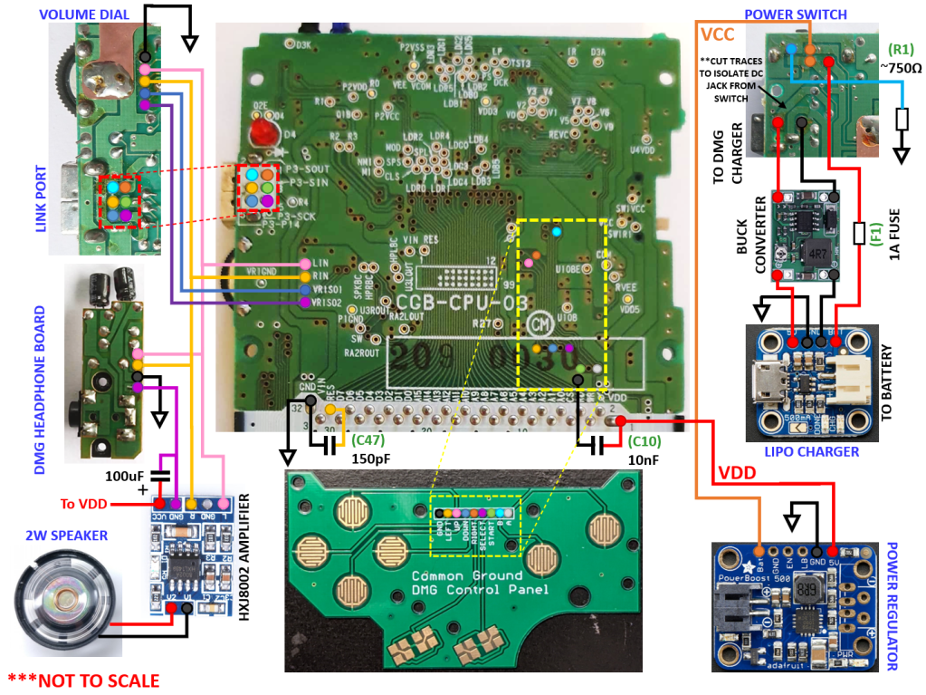
The blue wires there indicate a bit of foreshadowing! Ok, quick initial tests show everything working as it should. Now, I’ll go over how I cut up the DMG motherboard to obtain the volume dial, EXT port, DC jack, and power switch that I’ll need.
Preparing the DMG Motherboard
The next step to take was to cut up the DMG motherboard to harvest it for parts. To get the parts I needed, I used a Dremel to cut portions out of the DMG board, and tried to keep at least one mounting hole from the PCB so I’d have an easier time lining it up and securing it to the case when I put it all back together. Before cutting it up, I removed parts from the board near the cuts I’d be making, like capacitors, resistors, and diodes. I saved two sections of the main board: a portion with the link port and volume dial, and a portion with the power switch and DC jack. Side note, in the picture of the back of the power switch/DC jack board, I added a 1kΩ resistor, which connects the “OFF” position of the switch to the GND pin of the DC jack (which connects to the rest of the board ground through another wire). This will show up on the schematic in a later section. I also removed the headphone breakout board that houses the headphone jack to save for later.


After using the Dremel, I cleaned up all the boards with some isopropyl alcohol. I also went around and removed all the remaining leads from parts I cut off, and cleaned up all the remaining solder on the board.
One thing to note, since I’m already talking about Dremeling up this PCB, I needed to isolate the DC jack from the power switch. The top of the board has a ground plane the whole width of the segment of board, so I had to cut a channel between the switch and DC jack. On the back of the board, there’s a trace that connects the power from the DC jack to the switch, so I made sure that was disconnected too.

In addition to removing these parts, I also removed the DMG’s cartridge connector using copper braid and some new solder. I’ll need to use this later on.
Preparing the GBC Motherboard
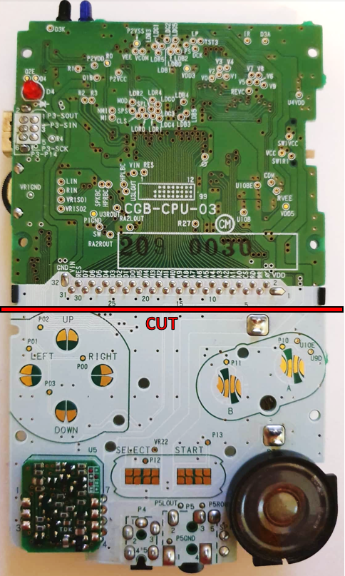
In order to start preparations for the parts I needed to remove, relocate, or replace on the GBC, I made up a handy little diagram for me to follow, shown below. Remember that I’ll have to remove the bottom half of the GBC to get it to fit inside the DMG case with the cartridge slot in the proper location.
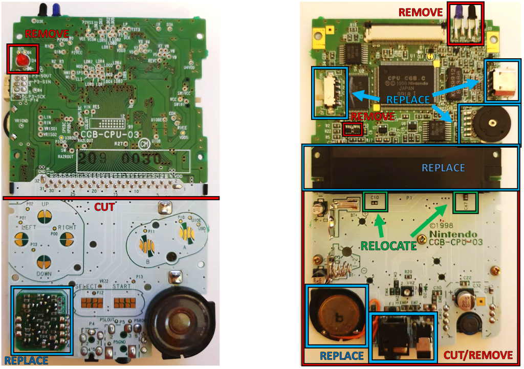
Before I dig into the real meaty part of this diagram, let’s go over the easy stuff first. The power switch, volume dial, EXT port, headphone jack, speaker, and cartridge connector will all be replaced with their DMG counterparts. The power LED will be replaced with a two-color LED wired off-board. The IR LED and IR sensor on the top of the board will be removed, as the DMG didn’t have this (and not many GBC games used it regardless). The AC adapter jack on the bottom of the board will be replaced with the DMG DC jack (at the top of the console), but will be used to charge the LiPo battery instead of powering the system. So, all of these parts will simply be removed for now.
There are a handful of other parts that I need to remove because of some notches I need to cut into the board, so I’ll go over those as well a bit farther down, with a more detailed photo.
Power Supply Board and Supporting Components
Future Nick here to note: on the final build, I replaced the GBC regulator board with an Adafruit PowerBoost 500 – easier and cheaper than designing my own regulator. The stock GBC regulator did work fine for the most part, but did introduce some noise into the audio circuit. So the first half of this section went ultimately unused, but the information is still helpful to understand the GBC.
The power supply board, underneath the D-pad in the left picture, needs to be carefully removed, because it will be used later on as the voltage regulator from the LiPo battery. It supplies the 5V rail, 13.6V rail, and -15V rail. The 13.6V and -15V rail are only used to power the LCD screen – but I am using an IPS screen, which only requires a 5V rail. Instead of re-wiring these two supplies back to the board where they will be going unused, I instead opted to tie them to GND using 10kΩ resistors, in order to keep them from floating to possibly high voltages. Those unused rails are on pins 5 and 6 of the power supply board, shown below.

C22 and C30 are also, therefore, not needed and can be removed. Next to this little board are two capacitors on the opposite side of the main PCB that need to be included – C31 and C32, a 4.7uF ceramic capacitor and a 100uF electrolytic capacitor, respectively. I have a ton of electrolytic capacitors, so I opted to only relocate the ceramic capacitor and just completely replace the electrolytic with one I had in my parts bin. Here’s what the board looks like with the capacitors relocated, as well as the 10kΩ resistors added to the unused supplies. In the pictures, the white wire is the battery voltage (VCC), the red wire is the 5V output (VDD), and the black wire is GND. Also note that pads 3 and 4 are both tied together on the board despite being on opposite sides of the board, so I only need one wire from either pad 3 or 4.


When I was removing the board, I accidentally ripped the 5V pad off of one of the sides of the board. No worries though, I just added a small wire to make sure the capacitor there had a good connection to the other side of the board. You’ll also see that the ceramic surface mount capacitor (C31) is between pins 1 and 3, soldered vertically on pad 1 with a wire connecting the top to pad 3.
Filtering Capacitor Relocation
Furthermore, C10 and C47 need to be removed and relocated as well. These bypass capacitors go to the power pin and reset pin on the cartridge connector. These are luckily really easy to relocate onto the top half of the board. C47 can be placed between the GND and /RES pins on the cartridge connector, and I found C10 is pretty easy to connect if you use the via shown in the picture above the /RD pin for the GND connection.


Cartridge Connector
After I had cut up the board (Future Nick here to tell you about it), I found that the cartridge connector on the GBC with the board attached didn’t fit very nicely in the slot. It caused the board to rise up a bit and hit the metal shielding on the cartridge connector. This is because the GBC connector (right) is thinner than the DMG connector (left).

It’s hard to take a good picture of how the GBC board sits like this so I’m not including it here. It basically tilts the whole board up a few degrees, and causes the board to contact the metal shielding. Instead of taping it all up and shoving cartridges into the connector anyway, which might over time loosen the connector pins, I decided to use a DMG cartridge connector in the GBC board. So I had to carefully remove the GBC’s cartridge connector. The pins line up perfectly, except pin 32 needs to kink out a bit. But that’s not a huge issue, and makes the whole board more secure in the long run, as the DMG’s plastic mounting will sit nicely on the screw holes for the DMG case.
Note though, I needed to trim the plastic posts on the bottom of the DMG connector so the whole thing sits flush against the board. (Apologies for the bad picture – I neglected to take one myself and it’s actually hard to find a picture of this thing off of the board)

Unnecessary LCD Components
Other than those things that I’ve mentioned, everything else on the bottom half can go. The remaining parts are either ferrites for noise filtering, or components that contribute to the LCD screen – but, as I mentioned, because I’m using an IPS screen, most of the LCD parts are unnecessary. All the supporting circuitry for the two now-unused power rails are unnecessary. Which brings me to U9 and U10, located just above the cartridge connector and below the power switch. These two chips are dual transistor devices, used for part of the LCD screen control.

Because the LCD’s 13.6V and -15V rails aren’t being used anymore, the parts that control the power going to the LCD screen are also unnecessary. However, some of the parts are located above the planned board cut line, while others are located below it and will be removed. Instead of worrying what will happen when some parts are removed and some aren’t, I opted to remove the two active parts left on the top half of the board that could feasibly pose an issue – U9 and U10. Removing the bottom half of the board, for example, will remove VR2. This could leave the base of the NPN device in U10 (pin 3) floating – which could cause excess power consumption, or even heat up the device itself. I don’t think this is necessarily likely, but it’s better to be safe than sorry. Removing these devices doesn’t hurt anything, at any rate.
Other Removable Parts
In order to fit the GBC board inside the DMG case, other than cutting the bottom half off, there are some notches I’ll have to make at the top to get it to fit properly. Luckily, many of the parts that could get in the way of this are also unnecessary, as they are used on the IR blaster and power LED, which are going to be unused – the parts are Q2, Q3, R7, and R8. Also, the DMG cartridge connector, being larger than the GBC one, hangs over some of the parts on the bottom of the top half of the board. Only a few are in the way, namely R2, R22, R5, and C36. Luckily these are all on the LCD circuit and can be removed without any issues. Finally, EM9 needs to be moved because I need to cut the board close to where the link port is mounted. And, one side of C9 will need to be reconnected to ground, as I will be cutting off the ground connection to it (but the part can stay on the board).

Here are the schematic locations of the removed/relocated parts.

I was able to relocate EM9 between the empty link port area and empty volume dial area – as it turns out, the mounting legs of the link port connect to pin 6, so putting the inductor between one of the mounting holes and GND (which has a connection conveniently located nearby underneath the volume dial) is the same as putting it between pin 6 and GND. The picture also shows the ground wire for C9.

Cutting the GBC Motherboard
In reality, when I did this project, I first wired things up to the uncut board (which is described in the next step) to verify everything worked properly just in case something I was doing would be irreparable after the board was cut up. But luckily, it worked just fine!
Anyway, the first cut is the largest. I basically cut across the bottom edge in a straight line, just above the BT+ terminal. This will make the board fit in the top half of the DMG shell. Time for the most stressful part of the build.
Afterwards, I cleaned off all the dust with some isopropyl alcohol, and inspected the board for any lodged conductive bits. Then, I returned to my workbench and reassembled the IPS screen, power switch, and the battery, just to make sure nothing was damaged. Luckily, it survived the ordeal. Now, it’s time to cut it up even more. The board won’t fit in the back shell without some notches to allow for the screw holes, and there needs to be some clearance for the DMG parts to fit as well. The good news is though, all of the places I need to cut only contain non-essential traces, so I have a bit of freedom to make this fit nicely. Here’s where I cut notches, and a view of the front and back of the board with the copper exposed.


The purple cut is quite extensive. Here’s what it looks like after surgery, as well as a view in the case with the two DMG boards in their locations.


I iterated on this a few times, trimming parts of both the GBC and the two DMG boards here and there to provide enough clearance between the boards, and finally got it to fit nicely. I’ll be trimming off any loose metal or board material, and probably using Kapton tape on the edges of the board to keep things from shorting. I’ll also most likely secure the boards together with a bit of glue to keep things steady, once everything is wired up.
I was able to do all of these cuts without cutting off any crucial traces. There is one location where the trace going to pin 3 of the link port almost gets cut off, but I verified after the cuts that it was safe and I double checked with a meter. However, because I’m cutting off a return path for the ground plane, to play it safe I went ahead and re-wired up a connection from the edge of the board to the top. I don’t think this actually did much, but it’s not hard to take precautions!

Future Nick here again to inform you about an issue I had after cutting the board. When I went to rewire this up in the next step, I found that the speaker did not work anymore. Let out a terrible continuous whine. I could not locate the actual root cause of the issue, but my guess is that I damaged a part on the amplifier circuit (or the amplifier) that I couldn’t visually detect or I introduced some kind of ground loop or feedback nearby the speaker output that wasn’t there before. Strangely, but fortunately, the headphones worked without any issue. To me, this means the audio signal is fine, it’s just that the speaker output specifically has some kind of issue. In order to get around this, I am going to be modifying my original plans, and use an audio amplifier separate from the one on the GBC (I mentioned this earlier in the parts list at the beginning). These updated plans will be the default going forward, but I’ll discuss what I was originally planning later on.
Anyway, let’s get into where I connected things onto the GBC board now that it’s all cut up.
Wiring Parts to the GBC Motherboard
This diagram went through a few iterations, but this is what I ended up with.
A few notes about this diagram, and what it includes and what it does not:
- This image does not have the components necessarily in the spots they will end up within the DMG shell, it was just convenient to draw it this way.
- In the case of the relocated items – C10, C47, and F1 were taken directly from the bottom half of the GBC. R1 was replaced with a 1kΩ resistor I had in my parts cabinet.
- I do not show the LED replacement in this diagram, nor the screen and accompanying circuitry, but I will go over the wiring later on.
- For the EXT port and the DMG button board, I do not show direct wires, but rather indicate where the wires connect with colored dots, for readability.
- There are a few extra wires I had to add due to trimming the board to fit properly. I have mentioned a few of these already, but the rest will be discussed in their relevant sections.
So, let’s get into the wiring. In each section I’ll break down the connections in more detail. This isn’t in any particular order, and I won’t be actually wiring it together until the next sections where I discuss the placements of the different parts. This section is to explain where everything will be wired after the build is complete, and why I wired it as such.
Also, if I had to modify a section multiple times to get the result I wanted, I kept all of the failed methods in, to better explain my choices and findings.
Battery, and Battery Charging Circuit
Note that Lithium-ion/polymer batteries are very dangerous. KNOW AND FOLLOW PRECAUTIONS BEFORE USING THEM.
I have seen many DMG mods that use a USB-C to charge LiPo batteries. But, as I do not want to make any external modifications to the Game Boy, I’m going to use the DC jack to charge my battery. The jack accepts the Game Boy AC adapter. This outputs about 6V nominally. What I want to do is take this 6V and plug it into my battery charger, which will produce the proper voltage/current setpoints for the LiPo battery. Adafruit sells a pretty easy-to-use battery charging board, and I figured this was easier/cheaper than making my own board after pricing out the individual parts plus the PCB. Looking at the batteries, I opted to get a nice, beefy 2000 mAh one with built-in overcurrent, overcharge, and overdischarge protection. None of the (larger) batteries that Adafruit sells would fit natively in the battery compartment – but, I will detail the battery compartment modifications to make it all fit later on.
Note that while I’m assembling things, I always keep the battery unplugged. Don’t want to short anything on the boards accidentally.

I set this board up to charge at a bit less than 200 mA, just to be safe. The DMG AC adapter only outputs 250 mA maximum anyway. So from an empty battery, it’ll take a bit more than 10 hours to charge up all the way (tests ran after final assembly clock in at approximately 11 hours). I don’t think I’ll care about letting the Game Boy have to sit for a bit longer to charge up, and my instinct is that running this thing at full power should last me 10+ hours as it is (tests ran after final assembly, using a flash cartridge, clock in at approximately 14 hours). To get 200 mA, I soldered a 10kΩ resistor on the “500mA” pad, instead of shorting it. Check out the schematic:

SJ1 there is where I put the 10kΩ resistor. That makes a 12.5kΩ in parallel with a 10kΩ, to give an equivalent resistance of about 5.6kΩ.
Wiring the Two-Color LED
Another thing I changed on this battery charger board was the charging and charge complete LEDs. The STAT pin on the MCP73831 will pull to LOW logic when the battery is charging, and when it is full, it will instead pull to HIGH logic. That means LED1 is on when charging (red), and LED2 is on when finished (green). The two-color LED I bought has a common cathode – that is, both cathodes are connected together. In order to use one LED with the 5V supply from the GBC board (the red LED) and the other LED as a charge indicator (the yellow LED), this common cathode must be tied to GND. Unfortunately, this means the STAT pin needs to be HIGH logic in order to turn on the LED during the charging period – the opposite of how it normally operates. In order to fix this problem, I simply removed the LEDs from the charging board, and wired in an NPN transistor (2N3904, specifically) to invert the signal, and added the two-color LED like so:

So, when STAT is HIGH (battery is done charging), the NPN transistor will conduct, and the yellow LED will have both ends tied to GND. But, when STAT is LOW (battery is still charging), the NPN transistor will be off, and power flows from the same voltage on VDD, through the 1kΩ resistor, and through the yellow LED to indicate it is charging. So, there’ll be a wire coming off the LiPo charging board that’s connected to the collector of the NPN transistor, that I will then solder to the yellow LED. As for the red power LED, all I need to do there is solder a resistor from the anode to somewhere on the 5V power supply from the GBC board.
Wiring the Buck Converter
Ok, now that that’s out of the way, you might be wondering, hey, that text in the battery charger chip’s box says VDD is 3.75V to 6V. And if you look at the datasheet for the MCP73831, the battery charging chip that this board uses, the maximum supply voltage it can handle is 6V. Since the nominal voltage output from the AC adapter is 6V, it’s unacceptable to use it directly – you generally want a good amount of headroom, 50% extra would be ideal. The output on this power adapter isn’t tight (I measure anywhere between 6V and 8.5V with a meter!), and it isn’t meant to be, so I can’t use it without dropping it down a bit first.
In order to handle this varying input voltage, I will be using a buck converter to step down the voltage to keep it within range. This buck converter will only be active when charging, not during actual gameplay (I’m not using a charge-and-play regulator), so I don’t have to worry about it interfering with my electronics. Again, my original plan was to make this all on one circuit board, but these “eBoot Mini” converters on Amazon come out to only $1.50 each! And they have a tiny footprint too. You can’t beat that.

The only annoying part about this board is that you have to manually adjust the potentiometer to get the correct output voltage, and it’s VERY sensitive. Took me a bit of trial and error and some tweezers, but I got the potentiometer adjusted to output about 5V.
These buck converters are great for simple stuff, but I think some of the details from the datasheet are dubious. On the datasheet, it says to keep at least 10% load at all time. Buck converters (and many other DC-DC converters) have a discontinuous mode when the load on them isn’t high enough, and this means poor regulation. You can get the output to float too high in this case. Now, if I were to put 10% of the maximum load (3A) on this thing, that’s a full 300 mA continuously sourced from the 5V output – that’s a full 1.5 W! So instead, I just slapped a 500Ω resistor across the output terminals. That pulls about 10 mA continuously, or about 50 mW. I checked the voltage with a scope, even without adding that extra load, and the output is still a solid 5V either way. Better safe than sorry though.
So anyway, in summary, I will be using the power from the DC jack on the DMG (pin 1 is GND, pin 2 is 6V), through a buck converter to regulate to 5V. This 5V will pass to the battery charger (5V hole on the LiPo charger), and then charge the battery. The battery positive line (BAT on the LiPo charger) will go to a 1A fast-blow fuse (GBC used a 1A or 2A fuse), and ultimately to the power switch.

I will eventually be storing all of this (minus the DC jack, obviously) in the back shell, where the battery compartment used to be. I had to trim out a lot of it to get it to fit. I’ll show this later on.
An Important Note about Heating
These simple battery chargers are essentially linear regulators. That is, to get the correct voltage for charging the battery, the chip will absorb the energy necessary to drop the voltage down from the input to the correct output. The higher the drop, and the higher the charging current, the hotter the chip will get. I did some quick tests with a power supply, and found that with charging an empty battery (approx. 3V) with a solid input voltage of 5.3V, at maximum charge rate (500 mA), the board gets quite toasty! Not the best thing to have held up against a LiPo battery.
Luckily, with my lower charge rate (200 mA), the solid 5V input, and with some insulation from the Kapton tape I wrapped the board in, the temperature increase on the board is pretty minor. I checked at various stages throughout charging the battery, and could only slightly tell it was getting warmer.
All of this is to say, if you’re ever going to be using a rechargeable battery and you have a linear charger like this one, you might want to test it outside of your project first to make sure nothing gets too hot.
Power Switch
One of the most crucial parts of the builds, the DMG power switch, is straightforward to connect to the GBC motherboard, once you think about it a bit. These two switches are different from each other – the DMG power switch is a DPST-NO/NC switch, and the GBC power switch is a simple SPDT switch. What are these abbreviations? Let’s start with the DMG switch. DPST means “double pole single throw.” This means there’s two separate switches that are controlled by a single toggle. NO means normally open, and NC means normally closed. So, a DPST-NO/NC switch has one normally open and one normally closed switch. Here’s a graphical representation of what I mean.

As it is wired on the board, according to the schematic, when in the OFF position, battery power is removed from the main power supplies, and the switch connects the /RESET pin on the processor to GND in order to provide a fast way of killing the game while the power supplies discharge. When the switch is in the ON position, the batteries are just normally connected to the power supply, and the /RESET pin is tied to VCC through an on-board pull-up resistor to allow the game to run normally.
On the GBC, the power switch is an SPDT switch, or single pole double throw. This essentially means there is one input that can be connected to two outputs. The power switch will connect the main power supply of the board to the battery when it’s in the ON position, or through a pull-down resistor to GND for fast discharging in the OFF position. In this picture, the switch is turned OFF.

So, it’s luckily very easy to turn the DPST-NO/NC switch into a SPDT switch. All there is to do is connect pins 1 and 3 together on the DMG switch, and that will act as pin C on the GBC switch. Then wire DMG pin 2 to the battery positive terminal (with fuse in series!) and DMG pin 4 to the pull-down resistor. (On the DMG board I cut out, I used a through-hole resistor to replace R1, so I didn’t have to wire to the actual GBC board.)

Oh, one note about the power switch. The original DMG switch had a little piece of plastic that extended out to keep the cartridge in during gameplay. It also had the added effect of preventing you from playing anything other than Game Boy games on it. In the picture below, I’m using Game Boy games on the left, Game Boy Color games on the right. And you can see that the button is blocked by the GBC cartridge for the original model.

So I just have to cut off that segment of the switch that pops out when I turn the game on.
EXT Port
The other DMG-harvested mini-board that I have house the link port and the volume dial. The DMG model’s EXT port is a different size than the Game Boy Pocket, Color, and Advance consoles, but helpfully, the pinout is still the same for each port. This means I can simply wire the port to the correct pins on the GBC motherboard. Easy!
Note that the pin numbering alternates, so one row is 1, 3, and 5, and the other is 2, 4, and 6.

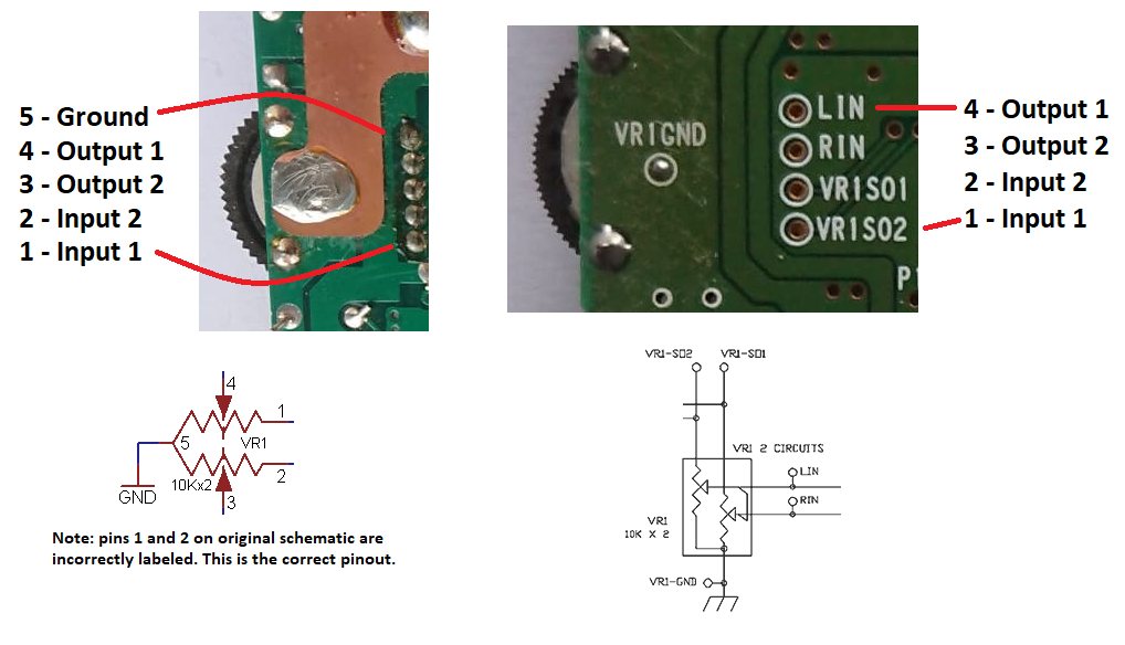
Volume Wheel
The volume dial is actually very straightforward, seeing that both the DMG and GBC wheels are five-pin devices. The GBC dial is essentially a slimmer version of the DMG one – same resistance and everything. And there are also very handily labelled test points available to wire to! The ground pin can go to VR1GND, or just any spot on the board that is connected to GND, whichever is more convenient.
Audio Components (First Pass)
These next few sections require a bit of explaining.
First things first – the GBC audio amplifier requires a VCC input – this is the unregulated voltage coming from the batteries. I believe this is used specifically for the speaker output, so that noise from the regulator doesn’t interfere with the audio signal coming out of it. The unregulated voltage is enough to drive the speaker, and it also is pretty clean because it’s just coming from the batteries – no switching noise at all. This VCC input was removed from the board when I cut notches into it, so I had to rewire it. I grabbed the voltage from the middle two pins of the power switch, and soldered it to these two vias next to C14, which connect to pins 4 and 14 on U3.

With that out of the way, onto the bigger picture. The headphones and speaker on the GBC are wired a bit differently than the DMG. Check out the schematic below, where the GBC headphone schematic is compared to the DMG headphone board (apologies for the janky hand-drawn DMG schematic, I wanted to add my own notes):

The “B” next to L1 indicates that this pin is labelled “B” on the board. The bottom wire connected to pin 3 of the headphone jack is the lone white wire.
Driving a speaker is pretty easy – the audio driver line is connected to the speaker and the other side is wired to GND. It is important, though, that somewhere in this audio path is a decoupling capacitor. Capacitors block DC components of signals, and if a DC voltage was applied to a speaker coil (which is low impedance), then the coil could become damaged due to too much power being dissipated within it. The audio signal only needs to be an AC waveform to make noise. If you notice, C38 on the GBC is responsible for decoupling the DC component from both the speaker AND the headphone jack (both left and right channels), whereas the DMG board has decoupling capacitors for both the left and right channels, as well as a separate capacitor for the speaker (not shown). Both are perfectly acceptable ways to wire it up, because the DC component will be blocked on every channel in both cases.
As for the headphone jacks themselves, they operate nearly identically to each other, with the only difference being their pinout. It appears pins 3 and 5 are swapped between them, but otherwise, everything is the same. Pin 3 on the DMG jack is connected to an internal switch that is normally closed (NC), which shorts pins 3 and 4 together (which is tied to GND). When an audio plug is inserted, this switch opens, and pin 3 is disconnected from GND. This is how the Game Boy knows when headphones are plugged in.
The GBC speaker, C38, EM1-EM5, and the headphone jack are all located on the bottom half of the GBC motherboard that will be removed. Luckily, none of these parts are needed if I wire up the DMG headphone board! I can simply wire the left and right channels to the RA2-LOUT and RA2-ROUT vias (again, the left channel is the wire labelled “B” on the board), wire pin 1/4 to GND, and pin 3 (white wire on the DMG board) to the SW test point, which is responsible for switching between headphone and speaker output. Also, since C38 is removed, I can just add an electrolytic capacitor in-line with the DMG speaker, with one side connected to SPKOUT on the GBC board. The easiest way to grab this signal is by soldering on the top of C14.


UNFORTUNATELY, as mentioned earlier in this post, when I wired this up onto my cut GBC board, the speaker didn’t work. Before cutting, it worked fine, but now it lets out a terrible whining noise. Now, I don’t know if this is because of something I did, by cutting the board or by accidentally shorting something that killed the speaker output. After checking the cut areas of the board and figuring out if I cut anything off that I shouldn’t have, I came up empty handed. I did a number of troubleshooting steps, and found that, importantly, the headphones still worked. This tells me the audio signal coming from the processor, as in, the inputs to the amplifier RIN and LIN, were still clean and worked fine. Otherwise, the headphones wouldn’t sound clean! So I have to assume something is going on with the speaker output that’s causing it to sound terrible.
Audio Components (Second Pass)
In order to get around this problem, I had to modify my strategy a bit. I opted to use the HXJ8002 amplifier board, which will completely bypass the amplifier U3 on the GBC board (which means that wire to VCC is unnecessary, lol). I found a guide on imgur that shows how to use this board, but I’ll repeat it here. Crucially, the strategy is to take the input audio signal going to U3 and use that for the speakers and headphones, instead of using the output of U3 for this. This should alleviate the issue with the speaker I’m having, and give it a bit more volume.
Let’s look at the schematic of the audio signal again, with a bit more context.

In the schematic here, the audio signal comes from the main GBC processor on the far left. It passes each channel through an RC filter, and eventually through the voltage divider VR1. VR1 is the volume dial – all it does is scale the audio signal between 0% and 100% magnitude. Normally, this passes to the audio management chip U3, but if you see the LIN and RIN signals I’ve circled, what I’ll be doing instead is grabbing the audio from these points to use for the headphones and the speaker amplifier board. (I didn’t remove U3 or any downstream parts from the board, but they could be removed if I wanted to take them off)

Also note that this amplifier, just like the one on the GBC board, is powered by the unregulated, non-noisy VCC line. The really clever thing here is that the ground connection to the amplifier board is only connected when no headphones are plugged in. Because I’ve wired GND to pin 3 on the DMG headphone jack, this connection will only be completed as long as there are no headphones plugged in. Once the headphones are plugged in, this connection to GND gets broken, and it turns off the amplifier board (and thus, the speakers). This means that there’s always an audio signal going to the headphone jack, but if nothing is plugged in, then it doesn’t hurt anything.
The guide mentions that the speaker needs to be rated for 2W, rather than the 1W that the DMG speakers are (I think they’re 1W?). The Amazon page for the amplifier mentions that 8Ω speakers are 1.5W max, but it also mentions 1W on the page, so I don’t know what to trust! It’s not very well documented. But just to be safe, I got this speaker that is conveniently the same size as the DMG ones, but rated for 2W.
Ok, so the sound is a lot better. After a few tests, I found that adding an extra bulk capacitance across the VCC and GND pins on the amplifier board cleans up the sound even more, but a funny side effect happens. If I add too much capacitance across the power pins, the GBC will reboot when I unplug my headphones. I’m pretty sure this is because when the headphones are unplugged, the GND pin reconnects to the main power of the GBC, which causes the bulk capacitance to draw a slug of inrush current, lowering the supply voltage. I found that 470uF capacitance REALLY cleans up the audio, but causes this issue. Lowering it to 100uF still filters out most of the white noise coming from the speaker, while not causing the brownout. I also tried connecting the negative lead of the capacitor to a permanent ground location instead, so it wouldn’t have to recharge every time the headphones were removed, but this didn’t do much for the sound quality.
So, the sound is now clearer, and louder. But there’s still some white noise in the background, and it gets a bit buzzy when the volume is turned up loudly. I believe this is due to the regulator on the board. It seems some noise is getting coupled onto the board through the return line. So I’ll briefly talk about the regulator now.
Power Regulator (First Pass)
I already talked about how I put the necessary parts onto the GBC regulator board in one of the above sections, so this will be quite short. All that’s really needed is to connect pin 1 on the regulator to the middle pins (pins 1 and 3) on the DMG switch, connect pin 3 or 4 (GND, tied on-board) to ground somewhere on the GBC board, and connect the 5V output on pin 7 to VDD somewhere on the GBC board. For the VDD and GND connections, I used pins 1 and 32 on the cartridge connector, respectively.

Not shown here, but I did wrap this in Kapton tape as a precaution.
After testing the sound on the system, and fiddling with the audio amplifier, I determined this regulator board to be a likely cause of noise coupling into the audio output. The regulator is notorious for being pretty noisy, from what I’ve seen online, and it apparently has a relatively low switching frequency which is probably what’s causing the issues. So I opted to try replacing it with a more robust boost converter, now that I don’t need the unregulated higher voltage lines for the LCD screen.
Power Regulator (Second Pass)
I opted to use the Adafruit PowerBoost 500 for a replacement regulator. It’s a bit overkill, but I know Adafruit’s products work, and I figured if using this didn’t solve my audio issues, I could just use it for a different project, and maybe use some more functionality that the board offers. I was wary about boost converters I saw online that didn’t explicitly state it was usable with Lithium-ion/Polymer batteries. At full charge, these batteries can be as high as 4.2V, and if a regulator isn’t tuned well or designed well, boosting to a voltage that is just barely higher than the input voltage can cause noise issues and even instabilities or overshoots. Since this board was designed for use with these batteries (it even has a JST connector on it meant to connect to a battery) it’s a safe bet.

I ended up having to remove the JST connector from the board to get it to fit properly in the case. It was a tight squeeze. I also wrapped the whole thing in Kapton tape to keep it isolated from any possible contact with other boards inside the case.
Audio Components (Third Pass)
I found that connecting the power pin of the audio amplifier board directly to the 5V regulated line on the PowerBoost resulted in a better sound than wiring to the battery voltage. This is the opposite of my findings when using the GBC regulator. So I wired to that instead (as indicated in the main diagram). I’m not too sure why this is, maybe some noise is being emitted from the battery charger board, but I’m not going to argue with it.
Alright. Audio issues aside now. Let’s continue on.
Button Input Board
The DMG has buttons in slightly different places than where the GBC has them. Luckily, the function of the buttons on a Game Boy Color are very simple – they just short a line to GND to indicate to the processor that the button has been pressed.

Basically, each button has exposed copper traces that are a short distance apart. When the button is pressed, the back of the button pad shorts the two sides together, which then pulls the corresponding pin to GND to indicate a button press.

There exists a handy PCB that replicates the bottom half of the DMG’s LCD board where the buttons are housed. All I have to do is wire up this board to replace the GBC’s button inputs. All of the numbered pads in the schematic above that connect to the non-grounded side of each button input (P01, P02, etc.) are on the bottom half of the GBC board that I’m cutting off, so I have to find vias elsewhere on the board to use instead. There are multiple vias to choose from for each line, generally, but here are the ones I picked. Other than the eight buttons, a ground wire needs to be added as well, which can go anywhere on the board where there is a ground connection.

I didn’t add actual lines in the diagram showing the connections in order to keep the view clear. There are multiple other vias that can be used, but these seemed the most convenient, with plenty of clearance between solder points. I also didn’t bother to wire this up to test before cutting the board in half, since I’ve used the board before and I know it works.
IPS Screen and Brightness Button
Installing this IPS screen is pretty self explanatory – remove the LCD, and put the ribbon cable going from the screen PCB in where the old ribbon cable was. As previously mentioned, this screen only uses the 5V rail, not the 13.6V and -15V rails that the LCD used. The board itself has a few connections to enable the OSD functions, as well as two capacitive touch pads to cycle between brightness settings and color palletes. Here’s a view of the pads for the OSD inputs. The red wire at the top is the wire that goes to the capacitive touch sensor for the brightness setting. But I’ll be changing some things on this board.

OSD Inputs and Battery Indicator
For the OSD inputs, I soldered wires from the SEL pad to the select button, the A pad to the A button, and the B pad to the B button (as one would expect). If I press all three of those buttons, the OSD opens up and I can set things there. Some games, this is going to be a nuisance (like Link’s Awakening when I want to quick save) but I don’t see it being a huge issue, as I won’t need to press those buttons at the same time often enough anyway. I suppose I could change the B button to down or something, there’s no reason it has to be the buttons the pads on the board call out.
There is also a pad for the battery input, in order to display the battery level on the top of the screen. This normally measures the voltage of two double-A batteries in series, which is about 3V max (about 2V at empty). However, I’m using a LiPo battery, which has a max voltage of 4.2V (about 3.2V at empty). Luckily, the range of the LiPo battery voltage is offset for both min and max by 1.2V, so I just need to shift the battery voltage reading down 1.2V. An easy, albeit somewhat imprecise, way to do this is just use the forward voltage drop on diodes. The 1N4148 has a forward voltage of approximately 0.6V when the current is around 1mA. I can use a 2.5kΩ resistor, powered by the battery voltage (which is read after the switch, so it doesn’t constantly drain the battery), with two diodes in series, to get me that ~1mA. Then I can simply read the voltage across the 2.5kΩ to get a shifted battery voltage, and wire it to the BAT pad. It won’t be a perfectly constant voltage drop – at full charge, the current through the diodes will be greater than at low charge changing the voltage drop to vary slightly, but the difference is negligible, especially as the battery level isn’t that precise to begin with.

I ran a simulation in LTSpice and came up with 3.01V to 2.05V as the range of voltages across the 2.5kΩ resistor. That squares pretty close with two AA batteries in series, which according to this website would read 2V a bit before completely collapsing.
Well, that was more work and explaining than was probably worth. In the end, it appears the OSD will show a full battery at around ~2.7V anyway (when the LiPo battery is at ~3.9V, or approximately 80% full), but the important part is that when the battery is nearly dead, the OSD accurately shows an empty battery. Once the battery icon shows it is empty, the battery will die about 15 minutes later, I’ve found.
To keep this simple (but ugly), I just soldered the parts on the IPS driver board, and left a long wire for the eventual connection to the battery voltage. I wrapped it all in Kapton tape.

Replacing the Touch Pad with a Button
The touch pads are finnicky, and I didn’t see the need to use the color pallete swapping one too often. Both of the touch pad functions can be controlled via the OSD menu anyway. So I removed the color pallete one. But, as I mentioned previously, the space where the DMG’s contrast dial is located wasn’t being used for anything, so I opted to turn the brightness touch pad into a brightness button, held in place by a 3D printed bracket that I designed. I picked this button because it was the largest button I could find that would fit in this location, as well as having the largest travel distance (how far the button pushes in) of that series. Chosen for maximum satisfaction!

The chip that senses the touch pad is the TTP223. It’s a simple 6-pin device that has a single output on pin 1 that goes to the processor on the board – a toggle from logic LOW to HIGH indicates the touch pad has been activated. So, it’s rather easy to hijack this line and use a simple button input for it – all I have to do is remove the TTP223, add a pull-up resistor from pin 1 to VDD (separate from the main VDD on the GBC board, located on pins 4 and 5), and then wire up the normally-open push button between pin 1 and GND.

I wired up pins 1 and 3 together to give me more locations to solder things onto the common node at pin 1 (pin 3 was the touch pad input, which is removed).
Preparing the Top Half of the DMG Shell
Now that I’ve explained all the wiring, it’s time to get into the actual assembly! But there’s a few things I need to address first.
Expanding the Viewing Area
The Q5 IPS screen is actually wider than the original screen area will provide. So I will need to do some trimming along the edges to expand the viewing area. The product listing indicates that the window should be trimmed back by about 1mm. I opted for about 2, just in case. As long as I don’t remove too much of the border, it shouldn’t matter, as the lens will cover it up.


After cutting the area bigger, I trimmed away any burrs left over to let the screen sit flush against the surface.
IPS Screen and Brightness Button
As previously mentioned multiple times, the GBC doesn’t have a contrast dial like the DMG (well, that is supposed to be easily accessible anyway), so I’ll be mounting that brightness button I wired up earlier where the contrast dial used to be. I designed a simplistic bracket to hold the button in place where the contrast dial used to be, as well as hold the screen in place so it doesn’t rotate. The lines seen in the model are just artefacts from Tinkercad, they’re actually smooth. You can get the model from Thingiverse here.

I had to cut two of the centering posts to get this to fit nicely, but they’re not necessary for the IPS screen anyway. I also printed a cover to go on top of the button, so the button actually sticks out and fits flush in the space where the DMG contrast dial used to be. Without this cover, you’d have to jam your finger into the hole, and there’d be some empty space surrounding it.
After lining up the bracket, I secured it to the shell with a little bit of hot glue. The phrase “hot glue” might trigger a negative response in some people, but it’s really quite handy, and honestly in my opinion, not a bad option in the right applications and the right amounts. I’m not applying insane globs of it or anything, just enough to keep things held in place. Hot glue is nice because you can easily take it off if you need to fix something later on, which I needed to do a few times for one reason or another. It loosens up if you get some IPA on it, or if it heats up from a nearby soldering iron, so you just need to watch out for that. But most importantly – it’s an insulator! So you don’t have to worry about it causing things to short to different locations.
Anyway, once the bracket was held in place, I put the brightness button in the slot, soldered two long wires to it, and glued that down as well. With the bracket secured, and the button ready to go, I peeled off the protective layer for the screen lens and placed that on the shell, careful not to fingerprint up the interior screen. Then I peeled off the screen protector on the IPS screen and placed it carefully in the bracket. I secured it down with Kapton tape to keep it in place. An insulating layer came with the screen that adheres to the back, which is conductive. This is to keep the back of the screen from shorting anything out on the circuit board it connects to. So I placed that on as well.


Audio Amplifier and Speaker
The speaker I bought fits nicely in the designated speaker area on the DMG shell. Just had to put down some tape to keep it in place. I soldered the speaker terminals to the audio amplifier board where indicated. For the input to the amplifier, I left four long wires, one for each the left and right input, one connected to GND, and one connected to VDD. Then, I secured it to the opposite corner of the DMG front shell, which is empty. How convenient!
(This picture is missing the 100uF electrolytic capacitor on the power inputs to the board)

DMG Button Board (and Buttons)
For this board, I simply soldered nine long wires in each of the holes for stripping and soldering to the GBC board later. I also added a second wire in the Select, A, and B points so that I can wire these to the IPS driver board. I put the buttons in the front shell, along with the membranes, and then screwed in the button board.

Power LED
Pretty simple. For now, I glued it into the hole, soldered three long wires for each of the pins, and trimmed the excess leads. No picture for you!
IPS Driver Board
Up until this point, I had avoided soldering when things were placed within the shell. But for this board, I decided it’d be easier to go ahead and solder things in while everything was placed. Just had to be extra careful not to touch any of the plastic.
There are a few points on this board that actually connect to GND, which I used to my advantage (circled in red below).

This came in really handy. Note that I already had some things soldered in for using a button in place of a touch pad for the brightness control (discussed earlier). Here’s what I soldered onto this board:
- Brightness button: one side to pad 1 where the TTP223 used to be, and the other side to GND.
- Battery voltage scaler: scaled voltage output to BAT pad, other side of 2.5kΩ resistor to GND. Extra wire hanging for connection to the battery voltage later.
- OSD control: the SEL, A, and B pads wired to their respective buttons, using the extra wire I had soldered into the button input board.
- Power LED: used one of the ground connections for the common cathode.
Then I put down some Kapton tape to hold things in place. With that, the front half is ready to go. It looks a bit messy, with all the wires going everywhere (they’ll be soldered eventually), but everything is secured and properly protected.

Preparing the Back Half of the DMG Shell
The back half of the shell requires a bit more preparation work than the top half. It’s also where all the brains are going to be housed.
The Battery Compartment
Most of the battery compartment is going to be stripped down. You can see in the picture, I first removed all the battery contacts, cut up all the plastic ridges that hold the AA batteries in, and crucially cut a hole in the left side of the compartment for the battery to slot into safely.


I wired the buck converter to the battery charger board. I left the rest alone for now, because I plan on snaking through wires to connect to these boards. A note, I have the fuse in-line coming from the battery voltage on the charger board. All of the boards in here will be properly protected so nothing short circuits, using Kapton tape, which also helps insulate the boards from heating up the battery. But as I mentioned, the heat generation from these boards is pretty low anyway. Luckily, everything fits if oriented correctly, with enough space between the battery and the boards, and the battery compartment still closes cleanly.
Uh… Everything Else
Most of the rest of this is self-explanatory when following the diagram, since there aren’t many places for things to go other than where they obviously belong. Firstly, I soldered the DMG cartridge connector in the GBC board. Then, to make assembly easier, I put all the boards in place in the back shell, and added a few dabs of hot glue away from any potential solder points. I added some Kapton tape in various areas to make sure the boards stay isolated from each other, in the event they get pushed too close together, before I glued them together.

Then I wired everything up for the back half assembly, which is basically anything that I haven’t already mentioned – the headphone jack, volume dial, link port, power switch, and regulator. I just followed my wiring diagram, and used long enough wires with sufficient slack. I guess the only thing that doesn’t have a defined position is the regulator board, which I nestled on the side where the DMG’s power board used to fit (I had to trim away the little plastic holder, though).

Final Reassembly
Finally, I put the two halves side by side and assessed the situation. I wanted to leave enough slack for the wires, in the event I had to open this up to fix something. There’s plenty of space for the wires to safely sit between the two halves, so I’m not too worried about pinching anything, as long as I keep them away from screw holes and the button board posts.

Here’s what I wired first:
- All the buttons from the DMG control panel board.
- The left, right, VDD, and GND wires from the audio board (the GND on the audio board will be wired to pin 3 of the headphone jack).
- The red power LED, including a 500Ω resistor in series.
- The input to the battery voltage scaling circuit, which connects to pin 1 on the regulator board (connected at the middle pins of the power switch).
In addition to this, I snaked through the following wires to the battery compartment, to wire later on:
- Wire from the “ON” position of the power switch (the middle pins), to connect to the battery voltage from the charging board. (Note this is only active when the switch is turned on, so I don’t constantly drain the battery when it’s off.)
- GND wire from the power supply board, to connect to the GND on the charging board.
- Wire from the DC jack input, to connect to the buck converter input.
- GND wire from the DC jack, to connect to the GND on the buck converter.
- Wire from the yellow charging LED, to connect to the modified status pin on the charging board.
Once all of these wires were in place, I taped them down with more Kapton tape and a liiiittle bit of hot glue for strain relief on a select few, and to also keep them away from any pinch points to make reassembly easier.
Penultimately, I wired the battery charger and buck converter boards (without the battery connected, of course) in place in the back shell. Once it was all wired up, I wrapped that in Kapton tape again and nestled the boards in the battery compartment.
Finally, the IPS screen needs to be connected to the GBC board. This is quite a tight fit, so instead of just doing it directly, I opted to get a 50 pin FFC (flexible flat cable) extension. The one I got came with a 6-inch cable, which is pretty excessive, but it does get the job done and there’s ample room inside to place it. I will most likely replace this with a shorter one in the future.

After this was all connected, I carefully placed the two halves together, put the power switch and brightness button in place, and screwed it all back together. And, to complete it, I finally plugged the battery back in and closed up the battery compartment. Now, for the moment of truth.

Lessons Learned and Updates
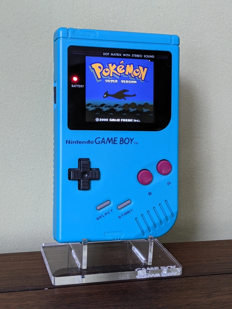
What a wild ride. But finally, I have my DMG Color final build. Despite this being overall easier than my last one, I think I was more stressed out about working on this one! But, ultimately, I came out with a much cleaner build, and hopefully one that’ll be more reliable. But, like any project, hindsight shows me a few things I could have done to make my life just a little bit easier and to make the build better.
- I probably didn’t have to cut the DMG board into so many pieces. The reason I had the pieces in the first place though, was because I had salvaged them from the previous project. But I probably could have gotten away with cutting off a larger board area that would keep things more secure. The GBC board had clearance on the top when put in the DMG shell that I could have used for more structural support.

- If I did this again, I’d check the speaker output way more often between board cuts, to really figure out what caused the speaker to make the original terrible noises in the first place. The additional audio amplifier was luckily an easy fix (after spending a decent amount of time troubleshooting). Maybe this speaker issue wouldn’t show up on every build. It might be nice to find a root cause at some point.
- Using the battery charger, buck converter, and regulator board separately came with some benefits, but if I wanted to be really proactive, I could have made my own power board that handled the battery charging and regulation by itself. That would probably be more expensive ultimately, but maybe a bit cleaner, and easier to fit.
- In general, using the LiPo battery itself introduced a lot of customization that I had to do. If I were to do this again, I might just keep the AA battery compartment in tact, and use rechargeable AAs instead. I could easily just close off the DC jack, or re-implement its original function. The final build would probably be a lot cleaner in this regard, at least internally. I would however need to put a sufficiently large diode drop in series with the battery voltage going to the regulator board, as four AAs would give 6V maximum, which is way above the expected maximum voltage rating for the board, and still decently higher than the voltage from a LiPo battery that it CAN handle.
- You know, thinking about this more, I might have a fun future PCB to create – shaped like the DMG board to fit in a DMG case, with DMG parts like the volume wheel and power switch, but with GBC guts. This way I don’t have to cut up boards, just transplant parts over, and even improve some things and introduce some customizability to it. But… that’s for another day.
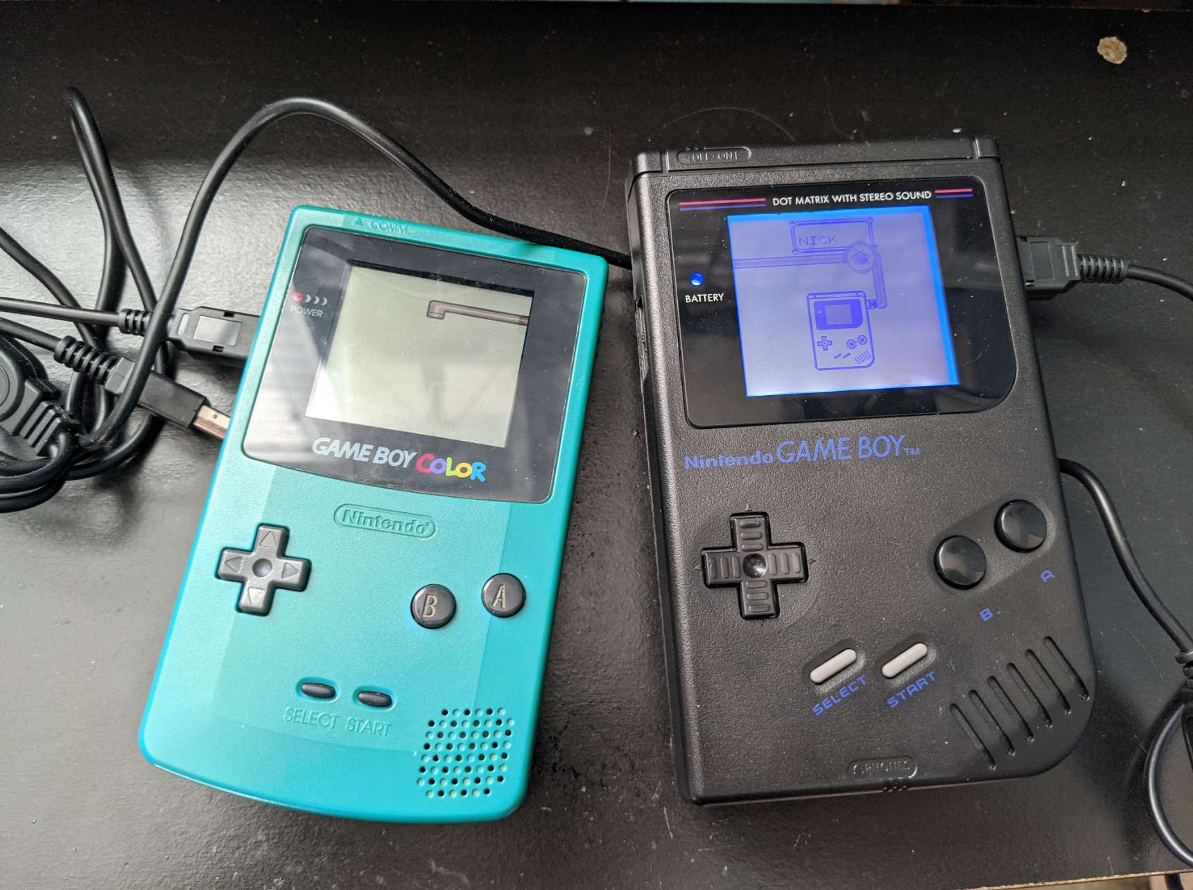
Despite all of the setbacks, I’m pretty proud of this build, and like my previous mod, I learned a lot about another piece of the Game Boy family. This is definitely going to become my default system for GB and GBC games. If you happen to find any errors or confusing points that you’d like clarified, feel free to tell me. I am not perfect, and I wrote this over the course of about two months in total, so I’m bound to have some inaccuracies somewhere. And I’ll be updating it if I come across any new issues, or decide to add any new features.
Thanks for reading!

References
- DMG schematics: https://gbdev.gg8.se/wiki/articles/DMG_Schematics
- DMG PCB layout: https://chipmusic.org/forums/topic/13608/dmg-main-board-schematic-circuit-arduinoboy/
- GBC schematics: https://console5.com/techwiki/images/e/e6/Nintendo_GBC_Schematic.png
- GBC board scans: https://github.com/Nintenfo/repository/tree/master/systems/GBC/documentation/schematics
- DMG and GBC pictures: https://gbhwdb.gekkio.fi/
- Adafruit LiPo charger schematic: https://cdn-learn.adafruit.com/assets/assets/000/017/043/original/adafruit_products_microlipo.png?1401477385
- DMG button PCB: https://circuit-board.de/forum/index.php/Thread/9847-Common-Ground-DMG-Control-Panel/?pageNo=3&s=5a6c507c679f2a41b528e672daa03713a41902d1
- My SP-in-a-DMG article: https://thepoorstudenthobbyist.com/2021/03/16/gba-sp-in-an-original-game-boy-case/
- Thanks to the gbdev and r/Gameboy Discord channels, for all the support and putting up with my semi-live-blogging

Beat me to it in the end – main problem I ran into was being completely unable to find a reasonably priced GBC where I live! Prices have jumped up horrendously even for poor condition examples so I’ve just sat and waited.
You’ve implemented much of what I was planning to do (probably in a cleaner way than I was going to anyway), though I was planning on ditching the GBC regulator board and just use the boost converter along with one of those USB-C battery boards (the ones that poke out the back of the battery compartment cover) – figure an aftermarket shell can take a little bit of modification 😉
LikeLike
Yeah I feel that! Luckily I was able to swap a working (but very dirty) GBC for a handful of my boards with someone I know. I’ve seen a few good deals on ebay here and there but you definitely have to be watching, they go fast.
Using a standard boost regulator certainly is an easy option! And the USB C would speed things up for sure. And most likely make it a lot cleaner. The battery compartment is a bit crowded on mine, which is fine, but it could be better.
I think ultimately, going with AA support would be the way I’d go next time though. I didn’t realize how light this one felt in comparison to a regular DMG with batteries. And it would really simplify the power stage.
If you want to share your project, let me know when you get yours built! I’d be interested to see.
LikeLike
[…] time, he’s revamped Nintendo’s classic handheld with the internals from its successor, the Sport Boy Colour (GBC). Clearly which means this new construct can’t play any GBA titles, […]
LikeLike
crazy job… nice!
LikeLike
[…] Game Boy Color in an Original Game Boy […]
LikeLike
[…] Game Boy Color in an Original Game Boy Shell […]
LikeLike
Hi, you wouldnt happen to still have the gameboy color pcb images locally? The link https://github.com/Nintenfo/repository/tree/master/systems/GBC/documentation/schematics is down.
LikeLike
Here ya go!
LikeLike
Absolutely amazing, thank you
LikeLike
Hello:
Because all operations of this screen kit can be done by OSD. So I want to change the newly added button used to adjust the brightness above your article to replace the SELECT button to call the OSD. May I ask if the connection method of the button is to connect one end to the SELECT pad of the screen circuit board, and solder the other end to GND?
Thank you.
(Please forgive me for using GOOGLE to translate from Chinese to English)
LikeLike
So, do you mean replace the select button with the rock-up button on the switch in the contrast dial?
LikeLike
Hello:
I mean in the “Replacing the Touch Pad with a Button” paragraph of the article, the button used to replace the touch pad. The original OSD Inputs is SELEST+A+B, changed to Button+A+B. The original GB SELECT button has not changed. Is this possible? Thanks
LikeLike
Oh yes, solder one side of the button to the select input and the other to GND. You will also need a pull-up resistor, 47K, soldered to the select input to the 3.3V supply on the GBC board
LikeLike
Thank you for this wonderful article and thank you for your reply.
LikeLike
Don’t suppose you have a schematic so that others can get a pcb printed do you?
LikeLike
I think you’re looking for the DMGC project: https://mousebitelabs.com/2022/10/25/the-game-boy-dmg-color-dmgc/
LikeLike