
- Day 1
- Introduction
- RISC-V
- ABIs
- OpenLANE
- Getting started with the platform
- Day 2
- Floorplan
- Floorplanning rules
- Need for library characterization
- Day 3
- SPICE simulations
- 16 step CMOS mask process
- DRC Checkers
- Day 4
- OpenSTA
- Clock Tree Synthesis
- Day 5
- Power Distribution Network
- Routing
- SPEF file generation
- Contact
- Acknowledgements
This course gives the basic overview of designing an IP(Intellectual Property) using the opensource tool OpenLANE from skywater foundaries in collaboration with google. The IPs which are being devolped will be of the scale of 130 nm. The designing rules are defined by the PDKs (Process Design Kit) which is not generally opensourced due to the integrity and also due to security concerns. We will work with a design reference namely picorv32a which is based on RISC-V ISA.The computers can only understand binary digits (that is 1s or 0s) to convert a program into that language we need an flow which takes in ISA converts it RTL then this is converted into layout. All these above steps require an interface and each interface needs to be designed such that the communication between each step is smooth.
./flow.tcl -interactive

RISC-V(stands for Reduced Instruction Set Computer Five) is an instruction set architecture which is open sourced for mainly learning and understanding of a computer architecture was devolped at University of California, Berkley. This ISA generally comes under little endian memory addressing mode or system which basically means Most Significant Bit is stored last and the Least Significant Bit is stored first. The memory in generally addresses a byte of data and there are only 32 regesters in RISC-V architecture meaning we can store the data in these regesters while running other commands such that it is efficent. The core(picorv32a) is a pre designed SoC which is generally used as a reference.
ABI stands for Application Binary Interface which is generally also called as System Call Interface is generally one of the interfaces which helps us run our commands on the hardware.
OpenLANE is an open source tool which basically runs all the program from RTL to GDSII. This tools helps us decide the ASIC Flow: RTL to GDSII(format of final layout) Processes are
- Synthesis (RTL in) RTL (HDL) gets converted into a circuit or digital design from a standard cell library. In openlane we have used
- OpenSTA : For post-synthesis analysis which is generally dumped onto the verilog file
- Yosys : It is used for mapping the RTL netlist
- abc : It generally uses PDK specification to map the cells accordingly
- Floor/Power Planning Chip-Floor-Planning: Partition the chip die between different system building blocks and place the I/O Pads. Marco-Planning: Generally the macros have to be fixed before we place any IPs
- Placement : Genererally done in two steps first it places them globally and then correctly places them to avoid any overlapping
- Ioplacer - It places the macros and connects I/O ports to the pins(pads)
- Clock-Tree Synthesis
- TritonCTS is the tool used for this step, It only creates a network of clock which is connected in routing step
- Routing : The most time consuming step as a result can be said as one of the most important step. We route the IPs and macros as well as connect them to their respective pins without violating any rules which can for example be routes which coinciede but have to be in differnet layers.
- Sign Off (GDSII out) : This step basically chhecks for any DRC errors or any such related errors.
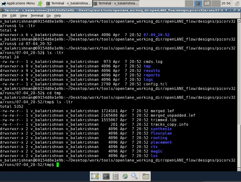
After the synthesis step we create a folder which stores all the data from RTL to GDSII for that specifications

package require openlane 0.9
prep -design picorv32a -tag foder_name
run_synthesis

- Core - The general idea is to encapsulate it with a die so that we get a protection. Intial netlist uses less space so that we can place other cells for optimisation. Dimensions of the chip mostly depends on the dimensions of the standard cells. (Width and Height generally determines the dimensions of the chip) We determine its ultilization factor from the following equations
Utilization Factor = (Area occuipied by Netlist)/(Total Area of the Core)
Ideally we go for a (50 - 60) % so that it is easier for the tools to work. The other factor is
(If it other than 1 it signifies rectangle)
-
Pre placed cells They can be macros or ips and alo are a part of the top level netlist. The location placing or arrangements of the cells are done only once because of their functionality which does not change, As a result they are placed before routing and placement of other cells
-
Decoupling capacitors are generally used incase the power supply for the gate falls under the undefined region in noise margin level which may cause it fall under both logic 1 or 0. It is a capacitor which is typically filled with a lot charge which will result in less loss of voltage/current.
-
Power planning If supply is being provided from one point we face two issues namely
- Ground bounce (discharging)
- Voltage droop (charging) Solution is to use multiple vdd vss lines creating power meshes which blocks of suc errors and allows the core to run smoothly.
We need to take care of below conditions to ensure that the floorplan does not have any errors :
- Giving shapes and sizes for the gates
- Binding the netlist with physical cells
- Libraries general hold the data for width delay and condtion of the cell which generally comes in different sizes (Bigger cells mean it runs faster)
- Depending on the I/O ports, Cells are placed to avoid any delays. Problems are generally solved by the technique called as optimize placement which basically estimates the length and capacitance on the basis of this information we try to insert repeaters to maintain the signal integrity.
run_floorplan

shows the value or the name asks for it
echo $::env(CURRENT_DEF) shows the which def file it is holding

we can make changes by using
set ::env(CLOCK_PERIOD) _value_

magic -T //loaction of magic T tech file// read lef //location of merged lef file// read def //location def
After running the command if we use the magic we can view this file which depiects the picture a floorplan with components placed globally

Ioplacer showing the data about the designs with respect to the config.tcl file , default file (Importantly the sky130a_fd_sc_hd file)


run_placement

It is important because it general holds all the data of a particular netlist which can be a cell or an IP. Depending on it we can determine the following conditions :-
- Logic Synthesis
- Floorplanning
- Placement
- Clock Tree Synthesis
- Routing
- STA
We generallly design a standard cell which can be placed in a library we take the inputs (from foundries) and accordingly we get PDKs(process design kits) which contains DRC & LVS rules, SPICE models files which gives us data on threshold voltage, capacitance etc and library, user-defined specs which specifies the cell height that is the gap between the power lines and ground lines , cell width and so on. (L = minimum feature size => lambda = L/2)
Circuit design which is followed by Layout design (art of layout design is eulers path and stick diagram which results in pmos network graph and nmos network), characterization and lastly outputs. We can also make custom layouts but it requires alot of specifications which may cause issues to the maker as it is not specified by them. CDL (circuit description language), GDSII(layout file),LEF(defines layout), extracted space netlist(.clr)(gives characterization flow)
- Reading-in the models
- Reading the extracted spice netlist
- Recognizing the behavoiur of the circuits
- Reading the sub circuits data and netlist
- Attaching the power sources
- Stimulus response checking
- And lastly necessary simulation command
SPICE decks for CMOS inverter and checks for component connectivity of source of pmos is connected to vdd and source of nmos is connected to capacitor. The below code is written for an inverter We analyse the data with respect to time and voltage These characteristics can be called as timing constrainsts a few below are examples of how they are cateogrised :-
- Slew low rise threshold
- Slew high rise threshold
- Slew low fall threshold
- Slew high fall threshold
- In rise thr
- In fall thr
- Out rise thr
- Out fall thr
** MODEL Descriptions **
** NETLIST Descriptions **
name_transistor drain gate source type w l
M1 out in vdd vdd pmos W=0.375u L=0.25u
M2 out in 0 0 nmos W=0.375u L=0.25u
cload out 0 10f
"dynamic simulation"
vin in 0 0 pulse 0 2.5 0(shift) 10p(rise) 10p(fall) 1n(pulse width) 2n(complete cycle length)
vdd vdd 0 2.5
vin in 0 2.5
** SIMULATION Commands**
.op
.dc Vin 0 2.5 0.05
.LIB "tsmc_025um_model.mod" CMOS_MODELS
.end


- Selecting a substrate which takes care of ptype,high resistivity(5~50omhs),doping lvl(10^15 cm^-3),orientation(100) and generally doping should be less than well doping.
- Creating active region for transistors which is done by growing a SiO240nm and Si3N4 80nm
- n well(pmos) and p well(nmos) which are created by ion implantation process
- Formation of gate which is very important as it controls threshold voltage
- Factors effecting gate doping concentration and oxide concentration
- Lightly Doped Drain (LDD) formation There are mainly 2 reasons why we need n- and p-
- Hot electron effect
- High energy carrier (breaks the Si-Si bonds)
- Source and Drain formation a thin layer of oxide for avoiding ion going into the substrate helps in randomize the direction of ions
- Generating contacts which form a means of communication between layers
- Higher level metal formation for proper contacting requirements i/o msut line on intersection hor width odd multiple hor pitch height odd multiple of ver pitch


We can check for drc errors by using the magic tool in which we have in built functions which can guide us to the error if and only if the configurations are speciefied accordingly

It is a tool which can be opened either using openroad (which is present inside openlane) or all by itself. This tool helps us reduce slack, find errors post synthesis which is helps the enginner debug any errors(bugs). STA stands for static timing anaylsis, generally slack means when the it is negative the output respresented is faster than the incoming input meaning the data shown at the output has not yet shown in the input which is flawed. That is why we generally prefer the slack to be positive or zero.
Before we run those commands on the opensta we need to first create the new lef file. The file can be replaced or sent to a new location by copying it
linux
write lef (in the magic tool window)
cp new_merged.lef to src location (where we have placed other important files for ease of communication)

The slack in the opensta tool after making changes that is by converting one buffer to another (meaning we increase the size to decrease the slew this does result in incremeant of cell size)
linux
replace_cell _cell number_ _with the type you want to replace_


After making all the adjustments we can run the command to force write the old synthesis.v file with new one
write //location of the synthesis.v file


It generally builds a sets of clock for a digital design circuit in a floorplan. This is a crucial step as it will determine whether we get a proper working CTS or not and also it will us the type of slack the core is running. CTS is generally done by the TritonCTS which is basically a part of openroad (openroad is intergrated into openlane)
run_cts
openroad
read_lef //location of lef file/merged.lef
read_def //location of current def file/picorv32a.xxx.def
write_db _name_.db
read_db _name_.db
read_verilog //location/picorv32a.synthesis_cts.v
read_liberty $::(LIB_SYNTH_CELL)
link_design picorv32a
read_sdc //location/xx.sdc
set_propagated_clocks [all_inputs]
report_checks //all the parameters you need
After we run the placement and clock tree synthesis we find that we have a positive slack this is due to the fact we have included standard cell library and also linked it to picorv32a core (inside the openroad)

Now we include the pre-made slack of -0.12 into the synthesis file and run till cts so that we have a base idea of how the slacks are after you try to obtain a positive slack in the opensta toll itself

report_clock_slew -setup
report_clock_slew -hold

run_pnd
Generally after verifying all the post cts synthesis values and specifications we end up with the power network creation where in the power is distributed throught the mesh which is powered by the pins placed along the ASIC. The power is connected through I/O pins (pads internally) which makes the ASIC perform the tasks.

Routing is generally done globally and detailed
- Global is less time consuming but has a drawback of not being as accurate as detailed routing
- Detailed routing does take double the time but is very detailed as a result it can be said to accurate
echo $::env(ROUTING_STRATEGY)
run_routing //for the workshop we have run global routing with the mode at 0

python.3 main.py //loaction of lef/merged.lef //location of def/picorv32a.routing.def
SPEF stands for standard Parastic Exchange Format generally represents the data (which are generally parameters such as resistance, capacitance) of a chip of ASIC design. Openlane does not support SPEF Extractor we need to do it manually using python as the script language.

- Kunal Ghosh - Co founder (VSD Corp Pvt Ltd)
- Nickson Jose - VSD VLSI Engineer
- Praharsha Mahurkar - VSD TA
- Akurathi Radhika - VSD TA