ASIA ELECTRONICS INDUSTRYYOUR WINDOW TO SMART MANUFACTURING
ADEKA Boosts Pitch Leading-edge Semiconductor Memory
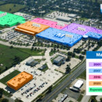
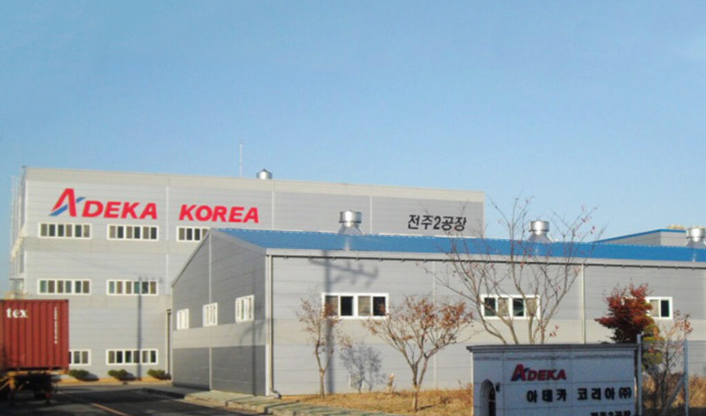
ADEKA CORPORATION has decided to expand the production facilities for high dielectric materials for leading-edge semiconductor memory. Particularly, the company will undertake this at its ADEKA KOREA CORPORATION. The production facility, with an investment of ¥2.1 billion, will begin commercial operation in FY2023.
Semiconductors are indispensable for an advanced ICT society. Most importantly, their market size is likely to grow to US$1 trillion by 2030. Semiconductor memory is a rapid technological innovation, such as miniaturization and 3D packaging, amid needs for higher capacity and reduced power consumption.
With these innovations, several new semiconductor materials are expected to be needed to accommodate new manufacturing processes and finer structures.
Aggressive Investment
Accordingly, high dielectric materials for advanced semiconductor memory, named ADEKA OCERA series is the No. 1 semiconductor materials in the world. Fuji Chimera Research Institute, Inc. made this conclusion in its 2020 Semiconductor Materials Market Status and Future Outlook.
ADEKA said it is investing aggressively in this product line because it is expected to be used in semiconductor processes for several more generations beyond the current generation as an indispensable product line for miniaturization.
Moreover, a plant is currently under construction to double production capacity in anticipation of future demand growth. This time, it will invest in the expansion of our product lineup, with a view to adopting new materials.
ADEKA Group aims to contribute to the realization of an advanced ICT society. Particularly, by strengthening and mutually collaborating with semiconductor materials-related R&D, production, and sales in Japan, Korea, Taiwan, and United States.
- Share: